# A B C D E F G H I J K L M N O P Q R S T U V W X Y Z

LINEAR TECHNOLOGY LTC3440 User's Manual

Summary

This highly efficient Buck-Boost DC/DC converter is ideal for portable electronics like MP3 players and digital cameras, providing reliable power conversion from wide-ranging battery voltages to a stable output. The comprehensive manual details the device's advanced capabilities, including single-inductor operation, programmable high switching frequencies (up to 2MHz), and energy-saving Burst Mode functionality. It is designed for engineers building sophisticated battery-powered instruments requiring maximum efficiency and extended operational longevity.
📄 Preview PAGE OF 20

Page 1 Text Content

LTC3440

Micropower Synchronous Buck-Boost DC/DC Converter

FEATURES DESCRIPTIO

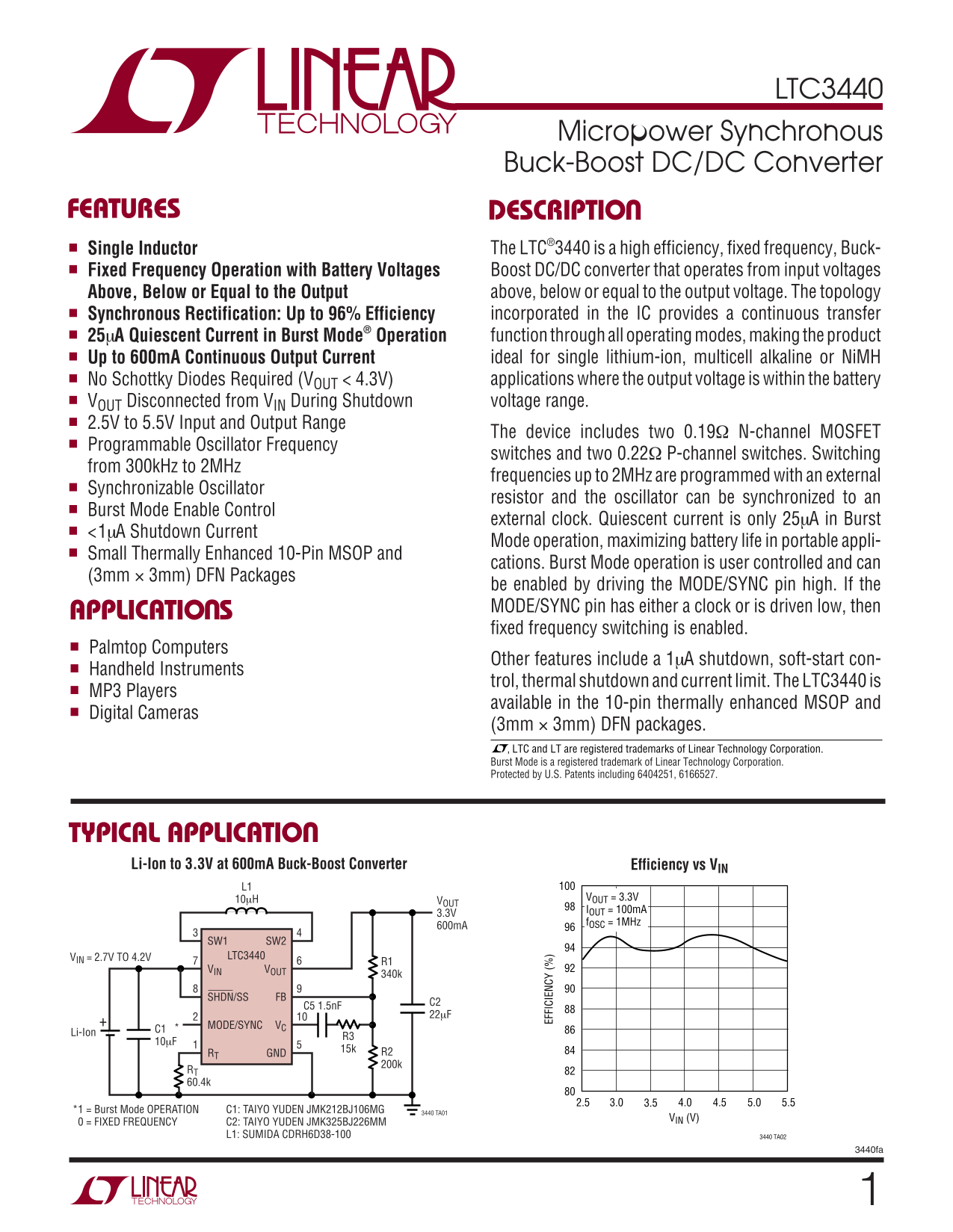
Single Inductor The LTC®3440 is a high efficiency, fixed frequency, Buck- Fixed Frequency Operation with Battery Voltages Boost DC/DC converter that operates from input voltages Above, Below or Equal to the Output above, below or equal to the output voltage. The topology Synchronous Rectification: Up to 96% Efficiency incorporated in the IC provides a continuous transfer 25µA Quiescent Current in Burst Mode® Operation function through all operating modes, making the product Up to 600m A Continuous Output Current ideal for single lithium-ion, multicell alkaline or Ni MH No Schottky Diodes Required (VOUT < 4.3V) applications where the output voltage is within the battery VOUT Disconnected from VIN During Shutdown voltage range.

2.5V to 5.5V Input and Output Range

The device includes two 0.19Ω N-channel MOSFET

Programmable Oscillator Frequency

switches and two 0.22Ω P-channel switches. Switching

from 300k Hz to 2MHz

frequencies up to 2MHz are programmed with an external

Synchronizable Oscillator

resistor and the oscillator can be synchronized to an

Burst Mode Enable Control

external clock. Quiescent current is only 25µA in Burst

<1µA Shutdown Current

Mode operation, maximizing battery life in portable appli-

EF FI CI EN CY

Small Thermally Enhanced 10-Pin MSOP and

cations. Burst Mode operation is user controlled and can

(3mm × 3mm) DFN Packages

be enabled by driving the MODE/SYNC pin high. If the MODE/SYNC pin has either a clock or is driven low, then

APPLICATIO S

fixed frequency switching is enabled.

Palmtop Computers

Other features include a 1µA shutdown, soft-start con-

Handheld Instruments

trol, thermal shutdown and current limit. The LTC3440 is

MP3 Players

available in the 10-pin thermally enhanced MSOP and

Digital Cameras

(3mm × 3mm) DFN packages. , LTC and LT are registered trademarks of Linear Technology Corporation. Burst Mode is a registered trademark of Linear Technology Corporation. Protected by U.S. Patents including 6404251, 6166527.

TYPICAL APPLICATIO

Efficiency vs VINLi-Ion to 3.3V at 600m A Buck-Boost Converter

10µH VOUT = 3.3V

IOUT = 100m A

f OSC = 1MHz

SW1 SW2 VIN = 2.7V TO 4.2V LTC3440

VIN VOUT

SHDN/SS FB

MODE/SYNC VC

Li-Ion

RT GND

RT 60.4k

*1 = Burst Mode OPERATION C1: TAIYO YUDEN JMK212BJ106MG 3440 TA01

VIN (V)

0 = FIXED FREQUENCY C2: TAIYO YUDEN JMK325BJ226MM L1: SUMIDA CDRH6D38-100 3440 TA02

3440fa

Page Summary Contents For LINEAR TECHNOLOGY LTC3440 User's Manual

Page 1 LTC3440 Micropower Synchronous Buck-Boost DC/DC Converter FEATURES DESCRIPTIO Single Inductor The LTC®3440 is a high efficiency, fixed frequency, Buck- Fixed Frequency Operation with Battery Voltages ...
Page 2 LTC3440 ABSOLUTE AXI U RATI GS (Note 1) VIN, VOUT Voltage........................................ –0.3V to 6V Operating Temperature Range (Note 2) –40°C to 85°C SW1, SW2 Voltage –0.3V to 6V Storage Te...
Page 3 EF FI CI EN CY LTC3440 ELECTRICAL CHARACTERISTICS The ● denotes specifications that apply over the full operating temperature range, otherwise specifications are at TA = 25°C. VIN = VOUT = 3.6V, RT = ...
Page 4 FR EQ UE NC (M Hz UT UR RE NT (µ A) LTC3440 TYPICAL PERFOR A CE CHARACTERISTICS VOUT Ripple During Buck, Switch Pins in Buck Mode Switch Pins in Boost Mode Buck/Boost and Boost Modes SW1 SW1 Buck 2V/D...
Page 5 DU TY YC LE LI NE EG UL AT IO (d B) LTC3440 TYPICAL PERFOR A CE CHARACTERISTICS Feedback Voltage Line Regulation Error Amp Sink Current PMOS RDS(ON) VIN = VOUT = 2.5V TO 5.5V VIN = VOUT = 3.6V VIN = V...
Page 6 LTC3440 PI FU CTIO S RT (Pin 1): Timing Resistor to Program the Oscillator ages over 4.3V, a Schottky diode is required from SW2 to Frequency. The programming frequency range is 300k Hz VOUT to ensure...
Page 7 LTC3440 BLOCK DIAGRA SW1 SW2 SW A SW D 2.5V TO 5.5V 2.5V TO 5.5V VOUT GATE DRIVERS SW B ANTICROSS SW C CONDUCTION ISENSE REVERSE AMP CURRENT LIMIT SUPPLY CURRENT LIMIT ERROR AMP LOGIC COMPARATORS OUTP...
Page 8 LTC3440 OPERATIO The LTC3440 provides high efficiency, low noise power Error Amp for applications such as portable instrumentation. The The error amplifier is a voltage mode amplifier. The loop LTC pr...
Page 9 LTC3440 OPERATIO The input voltage, VIN, where the four switch region begins 75% DMAX V4 (≈2.05V) is given by: BOOST A ON, B OFF BOOST REGION PWM CD SWITCHES DMIN OUT= V3 (≈1.65V) VIN BOOST FOUR SWITC...
Page 10 LTC3440 OPERATIO voltage from the error amp to determine the control mode, Burst Mode Operation to Fixed Frequency Transient therefore full-time 4-switch mode is required to maintain Response the Buck...
Page 11 LTC3440 OPERATIO SOFT-START A detailed diagram of this function is shown in Figure 5. The components RSS and CSS provide a slow ramping The soft-start function is combined with shutdown. When voltage ...
Page 12 LTC3440 APPLICATIO S I FOR ATIO Ripple = allowable inductor current ripple The output capacitance is usually many times larger in (e.g., 0.2 = 20%) order to handle the transient response of the conver...
Page 13 LTC3440 APPLICATIO S I FOR ATIO Output Voltage &gt; 4.3V Closing the Feedback Loop A Schottky diode from SW to VOUT is required for output The LTC3440 incorporates voltage mode PWM control. voltages o...
Page 14 LTC3440 APPLICATIO S I FOR ATIO traces and external components. Following the recom- POLE mendations for output voltage &gt;4.3V and input voltage &gt;4.5V will improve this condition. Additional shor...
Page 15 LTC3440 APPLICATIO S I FOR ATIO Simple Average Input Current Control INPUT_VOLTAGE A simple average current limit circuit is shown in 10µFV1 R1 Figure 10. Once the input current of the IC is above 0.5...
Page 16 LTC3440 TYPICAL APPLICATIO S 3-Cell to 5V Boost Converter with Output Disconnect 3-Cell to 5V Boost Efficiency 10µH VOUT VIN = 4.5V SW1 SW2 Burst Mode OPERATION VIN = 2.7V TO 4.5V LTC3440 VIN VOUT VIN...
Page 17 LTC3440 TYPICAL APPLICATIO S Efficiency of the WCDMA WCDMA Power Amp Power Supply with Dynamic Voltage Control Power Amp Power Supply VOUT = 3.3V – 1.7V • (VDAC – 1.22V) DAC VOUT = 3.4V IOUT = 100m A ...
Page 18 LTC3440 PACKAGE DESCRIPTIO DD Package 10-Lead Plastic DFN (3mm × 3mm) (Reference LTC DWG # 05-08-1699) (2 SIDES)2.15 ±0.05 (4 SIDES) (2 SIDES) PIN 1 PACKAGE TOP MARK OUTLINE (SEE NOTE 6) (DD10) DFN 11...
Page 19 LTC3440 PACKAGE DESCRIPTIO MS Package 10-Lead Plastic MSOP (Reference LTC DWG # 05-08-1661) (NOTE 3) (.0120 ± .0015) (.0197) (.0196 ± .003) TYP BSC REF RECOMMENDED SOLDER PAD LAYOUT DETAIL “A” (.118 ±...
Page 20 LTC3440 TYPICAL APPLICATIO Li-Ion to 3.3V at 600m A Buck-Boost Converter L1 Efficiency 10µH VOUT 3.3V 600m A220p F Burst Mode SW1 SW2 OPERATION LTC3440 R1 VIN = 2.8V TO 4.2V VIN VOUT VIN = 4.2V SHDN/S...

Manual Details

Brand Linear
Pages 20
File Size 222.22 KB
Published July 16, 2026
0 views

Enter the captcha to get the download link:

captcha

Frequently Asked Questions

Does it handle voltage differences between input and output?

Yes, the LTC3440 is a Buck-Boost converter that operates whether the input voltage is above, below, or equal to the output voltage.

What is the minimum standby current draw for battery longevity?

The shutdown quiescent current is less than 1µA, which helps maximize battery life in portable applications.

How can I customize the switching frequency?

You can program the oscillator frequency from 300kHz up to 2MHz using an external synchronizable resistor.

What is the maximum continuous output current it supports?

The device can handle up to 600mA of continuous output current, making it ideal for single lithium-ion or NiMH applications.