LINEAR TECHNOLOGY LTC3421 User's Manual
Summary
This high-efficiency synchronous boost DC/DC converter is engineered for reliable power management in portable, low-drain applications. Featuring up to 96% efficiency and true output disconnect capability, the LTC3421 maintains operation with ultra-low quiescent current (12mA) while providing robust power boosts for battery backup or handheld electronics. The accompanying manual provides comprehensive details on its programmable features—including customizable switching frequency and soft-start control—and includes detailed application circuits ideal for GPS receivers, cordless phones, and advanced battery management systems needing maximum longevity.
Page 1 Text Content
LTC3421
3A, 3MHz Micropower Synchronous Boost Converter with Output Disconnect
FEATURES DESCRIPTIO Synchronous Rectification: Up to 96% Efficiency The LTC®3421 is a high efficiency, current mode, fixed True Output Disconnect frequency, step-up DC/DC converter with true output dis- Inrush Current Limiting connect and inrush current limiting. The device includes a Very Low Quiescent Current: 12µA 0.10Ω N-channel MOSFET switch and a 0.14Ω P-channel Up to 1.5A Continuous Output Current synchronous rectifier. This product has the ability to sim- Fixed Frequency Operation Up to 3MHz ply program the output voltage, switching frequency, cur- 0.5V to 4.5V Input Range rent limit, soft-start, Burst Mode threshold and loop 2.4V to 5.25V Adjustable Output Voltage compensation with external passive components. Guaranteed 1V Start-Up
Quiescent current is only 12µA during Burst Mode opera-
Programmable Current Limit
tion, maximizing battery life in portable applications. The
Programmable Soft-Start
oscillator frequency can be programmed up to 3MHz and
Synchronizable Oscillator
can be synchronized to an external clock applied to the
Manual or Automatic Burst Mode® Operation
SYNC pin. An open-drain uncommitted low-battery com-
Low-Battery Comparator
parator is included. The part maintains operation in
<1µA Shutdown Current
applications with a secondary cell powering the output
1.22V Reference Output Voltage
voltage during shutdown.
Small (4mm × 4mm) Thermally Enhanced QFN
EF FI CI EN CY
Package Other features include: 1µA shutdown, antiringing control, thermal limit and reference output.
APPLICATIO S
The LTC3421 is available in a small 4mm × 4mm QFN Handheld Computers package.
Cordless Phones , LTC and LT are registered trademarks of Linear Technology Corporation.
Burst Mode is a registered trademark of Linear Technology Corporation.
GPS Receivers Battery Backup Supplies
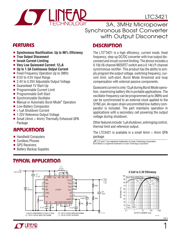
TYPICAL APPLICATIO
VIN 1.8V TO 3V 2-Cell to 3.3V Efficiency
SHDN VIN SW SW SW Burst Mode OPERATION
ENB VOUTS
3.3V VIN = 3V VIN = 2.4V
VREF VOUT 1.2A
VIN = 2V
LBI VOUT
CELLS LBO LTC3421 VOUT
SYNC FB
ILIM VC
BURST
SS RT GND PGND PGND PGND
VOUT = 3.3V 0.1µF 28k f OSC = 1MHz
C5: TAIYO YUDEN JMK325BJ226MM 3421 TA01 OUTPUT CURRENT (m A)
*LOCATE COMPONENTS CLOSE TO PINS
C1: TAIYO YUDEN JMK212BJ106MM L1: TDK RLF7030T-4R7M3R4 3421 G02
Page Summary Contents For LINEAR TECHNOLOGY LTC3421 User's Manual
Manual Details
| Brand | Linear |
|---|---|
| Pages | 16 |
| File Size | 234.45 KB |
| Published | June 16, 2026 |
Enter the captcha to get the download link:

Frequently Asked Questions
What is the maximum continuous output current?
The device can provide up to a 1.5A continuous output current.
Does the LTC3421 detect low battery conditions?
Yes, it includes an open-drain uncommitted low-battery comparator and maintains functionality during shutdown through a secondary cell.
What are the supported input voltage ranges?
The operational input voltage range is 0.5V to 4.5V (adjustable output voltage).
What package format is required for this device?
It is available in a small, thermally enhanced QFN package, measuring 4mm x 4mm.