# A B C D E F G H I J K L M N O P Q R S T U V W X Y Z

LINEAR Technology LTC2404 LTC2408 Data Sheet Manual

Summary

These ultra-low power, high-resolution Analog-to-Digital Converters (ADCs) are designed for demanding data acquisition applications requiring maximum precision and minimal latency. Featuring 4 or 8 channels and 24-bit accuracy, they utilize advanced delta-sigma technology with no missing codes and integrated digital filtering to resolve common signal offset issues. The comprehensive manual details specifications for various communication protocols (SPI, MICROWIRE), single supply operation (2.7V to 5.5V), and customizable inputs, making them ideal for instrumentation designers working on industrial control, gas analysis, and precision measurement systems.
📄 Preview PAGE OF 37

Page 1 Text Content

LTC2404/LTC2408

4-/8-Channel 24-Bit µPower No Latency ∆ΣTM ADCs

FEATURES DESCRIPTIO

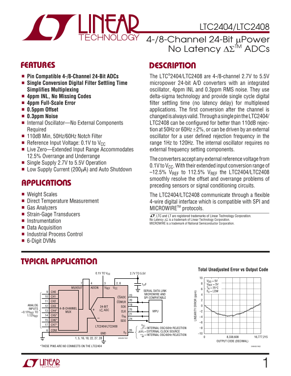
Pin Compatible 4-/8-Channel 24-Bit ADCs The LTC®2404/LTC2408 are 4-/8-channel 2.7V to 5.5V

Single Conversion Digital Filter Settling Time micropower 24-bit A/D converters with an integrated

Simplifies Multiplexing oscillator, 4ppm INL and 0.3ppm RMS noise. They use 4ppm INL, No Missing Codes delta-sigma technology and provide single cycle digital 4ppm Full-Scale Error filter settling time (no latency delay) for multiplexed 0.5ppm Offset applications. The first conversion after the channel is 0.3ppm Noise changed is always valid. Through a single pin the LTC2404/ Internal Oscillator—No External Components LTC2408 can be configured for better than 110d B rejec- Required tion at 50Hz or 60Hz ±2%, or can be driven by an external 110d B Min, 50Hz/60Hz Notch Filter oscillator for a user defined rejection frequency in the Reference Input Voltage: 0.1V to VCC range 1Hz to 120Hz. The internal oscillator requires no Live Zero—Extended Input Range Accommodates external frequency setting components.

12.5% Overrange and Underrange

The converters accept any external reference voltage from

Single Supply 2.7V to 5.5V Operation

0.1V to VCC. With their extended input conversion range of

Low Supply Current (200µA) and Auto Shutdown

–12.5% VREF to 112.5% VREF the LTC2404/LTC2408 smoothly resolve the offset and overrange problems of

APPLICATIO S

preceding sensors or signal conditioning circuits.

Weight Scales LI NE AR IT ER RO (p pm The LTC2404/LTC2408 communicate through a flexible

Direct Temperature Measurement 4-wire digital interface which is compatible with SPI and Gas Analyzers MICROWIRETM protocols. Strain-Gage Transducers , LTC and LT are registered trademarks of Linear Technology Corporation.

No Latency ∆Σ is a trademark of Linear Technology Corporation.

Instrumentation

MICROWIRE is a trademark of National Semiconductor Corporation.

Data Acquisition Industrial Process Control 6-Digit DVMs

TYPICAL APPLICATIO

Total Unadjusted Error vs Output Code

0.1V TO VCC 2.7V TO 5.5V

VDD = 5V

1µF VREF = 5V

ADCINMUXOUT VREF VCC TA = 25°C

SERIAL DATA LINK FO = LOW

MICROWIRE AND

CH1 CSADC

SPI COMPATABLE

CH2 CSMUX

ANALOG CH3

24-BIT SCK

INPUTS 4-/8-CHANNEL

CH4* ∆∑ ADC

–0.12VREF TO MUX CLK MPU –2

1.12VREF CH5* DIN

CH6* SDO

CH7* VCC

LTC2404/LTC2408

= INTERNAL OSC/50Hz REJECTION –8

= EXTERNAL CLOCK SOURCE

GND FO

= INTERNAL OSC/60Hz REJECTION

2404/08 TA01 8,338,608 16,777,215

OUTPUT CODE (DECIMAL)

*THESE PINS ARE NO CONNECTS ON THE LTC2404 2404/08 TA02

Page Summary Contents For LINEAR Technology LTC2404 LTC2408 Data Sheet Manual

Page 1 LTC2404/LTC2408 4-/8-Channel 24-Bit µPower No Latency ∆ΣTM ADCs FEATURES DESCRIPTIO Pin Compatible 4-/8-Channel 24-Bit ADCs The LTC®2404/LTC2408 are 4-/8-channel 2.7V to 5.5V Single Conversion Digital...
Page 2 LTC2404/LTC2408 ABSOLUTE MAXIMUM RATINGS (Notes 1, 2) Supply Voltage (VCC) to GND.......................–0.3V to 7V Operating Temperature Range Analog Input Voltage to GND –0.3V to (VCC + 0.3V) LTC240...
Page 3 LTC2404/LTC2408 CONVERTER CHARACTERISTICS The ● denotes specifications which apply over the full operating temperature range, otherwise specifications are at TA = 25°C. (Notes 3, 4) PARAMETER CONDITIO...
Page 4 LTC2404/LTC2408 DIGITAL I PUTS A D DIGITAL OUTPUTS The ● denotes specifications which apply over the full operating temperature range, otherwise specifications are at TA = 25°C. (Note 3) SYMBOL PARAME...
Page 5 LTC2404/LTC2408 TI I G CHARACTERISTICS The ● denotes specifications which apply over the full operating temperature range, otherwise specifications are at TA = 25°C. (Note 3) SYMBOL PARAMETER CONDITIO...
Page 6 ER RO (p pm ER RO (p pm ER RO (p pm LTC2404/LTC2408 TYPICAL PERFOR A CE CHARACTERISTICS Total Unadjusted Error Negative Extended Input Range (3V Supply) INL (3V Supply) Total Unadjusted Error (3V Supp...
Page 7 FU LL -S CA LE RR OR (p pm NU BE OF EA DI NG RM NO IS (p pm EF LTC2404/LTC2408 TYPICAL PERFOR A CE CHARACTERISTICS RMS Noise vs Reference Voltage Offset Error vs VCC RMS Noise vs VCC VCC = 5V VREF = 2...
Page 8 RE JE CT IO (d B) SU PP LY UR RE NT (µ A) RE JE CT IO (d B) LTC2404/LTC2408 TYPICAL PERFOR A CE CHARACTERISTICS Conversion Current vs Temperature Sleep Current vs Temperature PSRR vs Frequency at VCC ...
Page 9 LTC2404/LTC2408 TYPICAL PERFOR A CE CHARACTERISTICS IN (B IT S) Resolution vs Maximum INL vs Maximum Output Rate Output Rate VCC = 5V FO = EXTERNAL VREF = 5V (20480 × MAXIMUM F0 = EXTERNAL OUTPUT RATE...
Page 10 LTC2404/LTC2408 8- CH AN NE UX PIN FUNCTIONS A high on this pin also disables the SDO digital output. A is shifted out of SDO on the falling edge of SCK. For normal low-to-high transition on CSADC dur...
Page 11 LTC2404/LTC2408 APPLICATIONS INFORMATION Converter Operation Cycle CONVERT The LTC2404/LTC2408 are low power, 4-/8-channel delta- sigma analog-to-digital converters with easy-to-use CHANNEL SELECT (SL...
Page 12 LTC2404/LTC2408 APPLICATIONS INFORMATION Ease of Use VCC + 0.3V The LTC2404/LTC2408 data output has no latency, filter 9/8VREF VREF settling or redundant data associated with the conversion cycle. The...
Page 13 LTC2404/LTC2408 APPLICATIONS INFORMATION Bit 31 (first output bit) is the end of conversion (EOC) Bits 3-0 are sub LSBs below the 24-bit level. Bits 3-0 may indicator. This bit is available at the SDO...
Page 14 LTC2404/LTC2408 APPLICATIONS INFORMATION Channel Selection Table 3. Logic Table for Channel Selection CHANNEL STATUS EN D2 D1 D0 Typically, CSADC and CSMUX are tied together or CSADC All Off is invert...
Page 15 LTC2404/LTC2408 APPLICATIONS INFORMATION The selection of 50Hz or 60Hz rejection can also be made by driving FO to an appropriate logic level. A selection –70 change during the sleep or data output st...
Page 16 LTC2404/LTC2408 RE SO LU TI ON (B IT S) IN (B IT S) APPLICATIONS INFORMATION Using an External Clock for Faster Conversion Times The DC specifications are guaranteed for f EOSC up to a maximum of 307....
Page 17 LTC2404/LTC2408 APPLICATIONS INFORMATION is used as an end of conversion indicator during the shows the logic table for channel selection. In order to conversion and sleep states. select or change a p...
Page 18 LTC2404/LTC2408 APPLICATIONS INFORMATION 2.7V TO 5.5V VCC = 50Hz REJECTION VCC FO = EXTERNAL OSCILLATOR = 60Hz REJECTION LTC2404/LTC2408 VREF CSMUX CS TO VCC –0.12VREF CH0 CSADC TO 1.12VREF TO CH7 SCK...
Page 19 LTC2404/LTC2408 APPLICATIONS INFORMATION CSADC/ CSMUX SCK/CLK TEST EOC TEST EOC BIT26BIT28BIT29BIT30BIT31 BIT4BIT27 BIT0 SDO MSB LSB LSBEXRSIG DIN DON’T CARE D2 D1 D0 DON’T CAREEN CONVERTER CONV SLEEP...
Page 20 LTC2404/LTC2408 APPLICATIONS INFORMATION 2.7V TO 5.5V VCC = 50Hz REJECTION = EXTERNAL OSCILLATOR VCC FO = 60Hz REJECTION LTC2404/LTC2408 VREF CSMUX CS TO VCC –0.12VREF CH0 CSADC TO 1.12VREF TO CH7 SCK...
Page 21 LTC2404/LTC2408 APPLICATIONS INFORMATION to the SCK pin. This signal may be used to shift the Typically, CSADC remains LOW during the data output conversion result into external circuitry. EOC can be ...
Page 22 LTC2404/LTC2408 APPLICATIONS INFORMATION mode. However, certain applications may require an exter- develop a 2.5µV offset signal. For a reference voltage VREF nal driver on SCK. If this driver goes HI...
Page 23 LTC2404/LTC2408 APPLICATIONS INFORMATION power dissipation. A series resistor between 27Ω and 56Ω performance of the device. It simply results in an offset/ placed near the driver or near the LTC2404/...
Page 24 LTC2404/LTC2408 OF FS ET RR OR (p pm FU LL -S CA LE RR OR (p pm APPLICATIONS INFORMATION VCC = 5V CIN = 1µF VCC = 5V VREF = 5V CIN = 10µF VREF = 5V VIN = 0V VIN = 0V TA = 25°C TA = 25°C CIN = 0.1µF CI...
Page 25 LTC2404/LTC2408 FU LL -S CA LE RR OR (p pm FU LL -S CA LE RR OR (p pm APPLICATIONS INFORMATION Reference Current (VREF) constants tied to the reference input. If the capacitance at node VREF is small ...
Page 26 LTC2404/LTC2408 RE JE CT IO (d B) APPLICATIONS INFORMATION ANTIALIASING The LTC2408’s Resolution and Accuracy Allows You to Measure Points in a Ladder of Sensors One of the advantages delta-sigma ADCs...
Page 27 LTC2404/LTC2408 APPLICATIONS INFORMATION 47µF OPTIONAL LTC1634-2.5 GAIN BLOCK LTC1050 UP TO SEVERAL HUNDRED FEET. 5V ALL SAME WIRE TYPE OPTIONAL PROTECTION 2, 8 RESISTORS ADCINMUXOUT VREF VCC 5k MAX P...
Page 28 LTC2404/LTC2408 APPLICATIONS INFORMATION AV = 1, 2, 4...1283 LTC1050 0.1V TO VCC ADCINMUXOUT VREF VCC CSADC 10k20k CSMUX CH3 24-BIT 8-CHANNEL CH4 ∆∑ ADC 10k20k MUX CLK 10k20k SDO CH7 VCC LTC2408 10k20...
Page 29 LTC2404/LTC2408 APPLICATIONS INFORMATION noise bandwidth of the system to 6Hz. The noise band- The code begins by declaring variables and allocating four width of the LTC2408 without any input bandwid...
Page 30 LTC2404/LTC2408 APPLICATIONS INFORMATION DIN1 EQU $00 This memory location holds the LTC2408’s bits 31 - 24 DIN2 EQU $01 This memory location holds the LTC2408’s bits 23 - 16 DIN3 EQU $02 This memory ...
Page 31 LTC2404/LTC2408 APPLICATIONS INFORMATION * The SPI data transfer TRFLP1 LDAA #$0 Load accumulator A with a null byte for SPI transfer STAA SPDR This writes the byte into the SPI data register and star...
Page 32 LTC2404/LTC2408 APPLICATIONS INFORMATION * This example program loads multiplexer channels selection data into * either the LTC2408’s internal MUX or an external LTC1391 MUX. It then * transfers the L...
Page 33 LTC2404/LTC2408 APPLICATIONS INFORMATION ENLWMX TBA Restore contents of Accum. A ORAA #$08 Set the MUX’s ENABLE bit MUXSPI STAA SPDR Transfer Accum. A contents to SPI register to initiate serial trans...
Page 34 LTC2404/LTC2408 APPLICATIONS INFORMATION amplifier-based or self-contained instrumentation ampli- Two channels (CH3 and CH4) of the LTC2408 are used to fiers (also available from LTC) can be used with...
Page 35 LTC2404/LTC2408 APPLICATIONS INFORMATION These infrared thermocouples are self-contained: 1) they The photodiode chosen (Hammatsu S1336-5BK) pro- do not require external cold junction compensation; 2)...
Page 36 LTC2404/LTC2408 TYPICAL APPLICATION GUARD RING VOLTMETER INPUT 0.1%, 1W, 1000 WVDC ELECTROMETER 1m V TO 1000V INPUT R2 (p H, PIEZO) 4.7k LT1793 0V TO 5V –60m V TO 4V LT1236CS8-5 OUT IN 8V5V MAX 10µF G...
Page 37 WWW.ALLDATASHEET.COM Copyright © Each Manufacturing Company. All Datasheets cannot be modified without permission. This datasheet has been download from : www.All Data Sheet.com 100% Free Data Sheet S...

Manual Details

Brand Linear
Pages 37
File Size 362.87 KB
Published June 16, 2026
1 views

Enter the captcha to get the download link:

captcha

Frequently Asked Questions

What is the required single supply voltage range for operation?

The converters operate on a single supply of 2.7V to 5.5V.

Are there any latency issues or data delays after a conversion cycle?

No, it uses No Latency DS technology, meaning the first converted reading is always valid immediately.

Which communication protocols are supported for data acquisition?

It communicates through a flexible digital interface compatible with SPI and MICROWIRE protocols.

What is the operating temperature range difference between variants I and C?

The 'I' versions operate from -40°C to 85°C, while the 'C' versions are rated from 0°C to 70°C.