LINEAR TECHNOLOGY LTC2053 LTC2053-SYNC User Guide and Manual
Summary
The LTC2053 is a high-precision instrumentation amplifier designed for advanced data acquisition, offering rail-to-rail input/output and zero-drift performance. It features user-adjustable gain via external resistors and supports single or dual supply operations. The comprehensive manual details its electrical specifications, various mounting packages (MS8 and DFN), and typical use cases in medical instruments, electronic scales, and strain gauge applications, making it ideal for professional engineers requiring reliable, high-resolution signal conditioning.
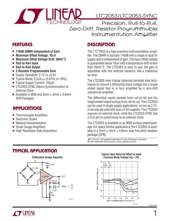
Page 1 Text Content
LTC2053/LTC2053-SYNC Precision, Rail-to-Rail,
Zero-Drift, Resistor-Programmable
Instrumentation Amplifier
FEATURES DESCRIPTIO 116d B CMRR Independent of Gain The LTC®2053 is a high precision instrumentation ampli- Maximum Offset Voltage: 10µV fier. The CMRR is typically 116d B with a single or dual 5V Maximum Offset Voltage Drift: 50n V/°C supply and is independent of gain. The input offset voltage Rail-to-Rail Input is guaranteed below 10µV with a temperature drift of less Rail-to-Rail Output than 50n V/°C. The LTC2053 is easy to use; the gain is
2-Resistor Programmable Gain adjustable with two external resistors, like a traditional Supply Operation: 2.7V to ±5.5V op amp.
Typical Noise: 2.5µVP-P (0.01Hz to 10Hz)
The LTC2053 uses charge balanced sampled data tech-
Typical Supply Current: 750µA
niques to convert a differential input voltage into a single
LTC2053-SYNC Allows Synchronization to
ended signal that is in turn amplified by a zero-drift
External Clock
operational amplifier.
Available in MS8 and 3mm × 3mm × 0.8mm
IN PU OF FS ET OL TA GE (µ V) The differential inputs operate from rail-to-rail and the
DFN Packages
single ended output swings from rail-to-rail. The LTC2053 can be used in single supply applications, as low as 2.7V.
APPLICATIO S It can also be used with dual ±5.5V supplies. The LTC2053
requires no external clock, while the LTC2053-SYNC has
Thermocouple Amplifiers
a CLK pin to synchronize to an external clock.
Electronic Scales
Medical Instrumentation The LTC2053 is available in an MS8 surface mount pack- Strain Gauge Amplifiers age. For space limited applications, the LTC2053 is avail- High Resolution Data Acquisition able in a 3mm × 3mm × 0.8mm dual fine pitch leadless package (DFN). , LTC and LT are registered trademarks of Linear Technology Corporation. All other trademarks are the property of their respective owners.
TYPICAL APPLICATIO
Typical Input Referred Offset vs Input
Differential Bridge Amplifier Common Mode Voltage (VS = 3V) 3V
VS = 3V
0.1µF VREF = 0V
TA = 25°C
LTC2053 OUT
GAIN = 1+
2053 TA01
INPUT COMMON MODE VOLTAGE (V)
2053 TA01b
2053syncfb
Page Summary Contents For LINEAR TECHNOLOGY LTC2053 LTC2053-SYNC User Guide and Manual
Manual Details
| Brand | Linear |
|---|---|
| Pages | 16 |
| File Size | 227.61 KB |
| Published | June 05, 2026 |
Enter the captcha to get the download link:

Frequently Asked Questions
What are the operating temperature ranges for different packages?
The LTC2053I is -40°C to 85°C, while the LTC2053H handles –40°C to 125°C. The MS8 package can operate from –65°C to 150°C.
Can I use this device in single-supply or dual-supply applications?
Yes, the LTC2053 supports single supply operations as low as 2.7V and can also be used with dual ±5.5V supplies.
Does the unit require an external clock signal?
The standard LTC2053 does not require an external clock. However, the LTC2053-SYNC version has a CLK pin for synchronization to an external clock.
What is the guaranteed Common Mode Rejection Ratio (CMRR)?
For the LTC2053C/LTC2053C-SYNC, the CMRR is typically 113 dB at certain operating ranges.