# A B C D E F G H I J K L M N O P Q R S T U V W X Y Z

LINEAR TECHNOLOGY LTC3704 Specifications and User Guide

Summary

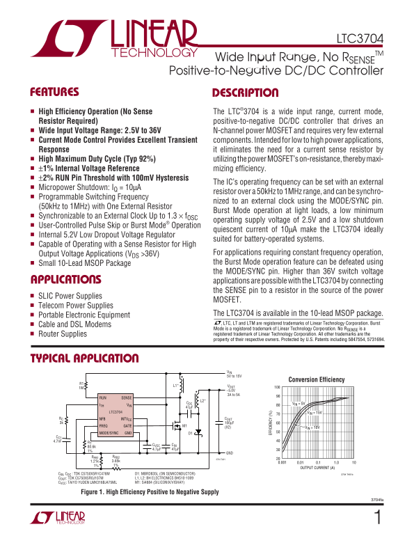
The LTC3704 is a high-efficiency positive-to-negative DC/DC controller designed for power applications ranging from low-power battery systems to high-capacity telecom equipment. It features an ultra-wide input voltage range (2.5V to 36V) and eliminates the need for a current sense resistor, maximizing efficiency with its integrated Power MOSFET. This manual provides detailed specifications and application guidance on utilizing programmable switching frequencies and advanced low-power modes, making it ideal for portable electronic devices and demanding power supplies.
📄 Preview PAGE OF 28

Page 1 Text Content

LTC3704 TM

Wide Input Range, No RSENSE

Positive-to-Negative DC/DC Controller

FEATURES DESCRIPTIO High Efficiency Operation (No Sense The LTC®3704 is a wide input range, current mode, Resistor Required) positive-to-negative DC/DC controller that drives an Wide Input Voltage Range: 2.5V to 36V N-channel power MOSFET and requires very few external Current Mode Control Provides Excellent Transient components. Intended for low to high power applications, Response it eliminates the need for a current sense resistor by

High Maximum Duty Cycle (Typ 92%) utilizing the power MOSFET’s on-resistance, thereby maxi- ±1% Internal Voltage Reference mizing efficiency.

±2% RUN Pin Threshold with 100m V Hysteresis

The IC’s operating frequency can be set with an external

Micropower Shutdown: IQ = 10µA

resistor over a 50k Hz to 1MHz range, and can be synchro-

Programmable Switching Frequency

nized to an external clock using the MODE/SYNC pin.

(50k Hz to 1MHz) with One External Resistor

Burst Mode operation at light loads, a low minimum

Synchronizable to an External Clock Up to 1.3 × f OSC

operating supply voltage of 2.5V and a low shutdown

User-Controlled Pulse Skip or Burst Mode® Operation

quiescent current of 10µA make the LTC3704 ideally

Internal 5.2V Low Dropout Voltage Regulator

suited for battery-operated systems.

Capable of Operating with a Sense Resistor for High

Output Voltage Applications (VDS >36V) For applications requiring constant frequency operation, Small 10-Lead MSOP Package the Burst Mode operation feature can be defeated using

EF FI CI EN CY

the MODE/SYNC pin. Higher than 36V switch voltage APPLICATIO S applications are possible with the LTC3704 by connecting the SENSE pin to a resistor in the source of the power

SLIC Power Supplies

MOSFET.

Telecom Power Supplies

Portable Electronic Equipment The LTC3704 is available in the 10-lead MSOP package. , LTC, LT and LTM are registered trademarks of Linear Technology Corporation. Burst

Cable and DSL Modems

Mode is a registered trademark of Linear Technology Corporation. No RSENSE is a Router Supplies registered trademark of Linear Technology Corporation. All other trademarks are the property of their respective owners. Protected by U.S. Patents including 5847554, 5731694.

TYPICAL APPLICATIO

VIN 5V to 15V

Conversion Efficiency

L1* VOUT

–5.0V 3A to 5A

RUN SENSE

CDC VIN = 5V

ITH VIN

LTC3704 VIN = 15V

RC NFB INTVCC COUT 3k 100µF

FREQ GATE M1 (X2)

VIN = 10V

MODE/SYNC GND D1

CC1 4.7n F RT

CVCC CIN

RFB1 RFB2

3704 TA01

OUTPUT CURRENT (A)

CIN, CDC : TDK C5750X5R1C476M D1: MBRD835L (ON SEMICONDUCTOR) 3704 TA01b COUT: TDK C5750X5R0J107M L1, L2: BH ELECTRONICS BH510-1009 CVCC: TAIYO YUDEN LMK316BJ475ML M1: Si4884 (SILICONIX/VISHAY)

Figure 1. High Efficiency Positive to Negative Supply

3704fa

Page Summary Contents For LINEAR TECHNOLOGY LTC3704 Specifications and User Guide

Page 1 LTC3704 TM Wide Input Range, No RSENSE Positive-to-Negative DC/DC Controller FEATURES DESCRIPTIO High Efficiency Operation (No Sense The LTC®3704 is a wide input range, current mode, Resistor Required...
Page 2 LTC3704 ABSOLUTE AXI U RATI GS PACKAGE/ORDER I FOR ATIO (Note 1) VIN Voltage –0.3V to 36V TOP VIEW INTVCC Voltage –0.3V to 7V RUN SENSE ITH VIN INTVCC Output Current 50m A NFB INTVCC FREQ GATE GATE Vo...
Page 3 LTC3704 ELECTRICAL CHARACTERISTICS The ● denotes specifications which apply over the full operating temperature range, otherwise specifications are at TA = 25°C. VIN = VINTVCC = 5V, VRUN = 1.5V, RFREQ...
Page 4 NF VO LT AG (V Bu rs t M od (µ A) SH UT DO OD (µ A) LTC3704 TYPICAL PERFOR A CE CHARACTERISTICS NFB Voltage vs Temp NFB Voltage Line Regulation NFB Pin Current vs Temperature FB LT AG (V (m A) SH UT D...
Page 5 IN TV OL TA GE (V GA TE RE QU EN CY (k Hz RU TH RE SH OL DS (V LTC3704 TYPICAL PERFOR A CE CHARACTERISTICS RUN Thresholds vs VIN RUN Thresholds vs Temperature RT vs Frequency 1.5 1.40 IN TV OL TA GE (...
Page 6 LTC3704 PI FU CTIO S RUN (Pin 1): The RUN pin provides the user with an operating frequency to an external clock. If the MODE/ accurate means for sensing the input voltage and pro- SYNC pin is connect...
Page 7 LTC3704 BLOCK DIAGRA BIAS AND SLOPE START-UP C2 COMPENSATION CONTROL 100m V HYSTERESIS FREQ VIN (1.348V RISING) OSCV-TO-I MODE/SYNC INTVCC 50k LOGIC NFB 200k BUFFER PWM LATCH SENSE BURST CURRENT COMPA...
Page 8 LTC3704 OPERATIO Main Control Loop The nominal operating frequency of the LTC3704 is pro- grammed using a resistor from the FREQ pin to ground The LTC3704 is a constant frequency, current mode and can...
Page 9 LTC3704 OPERATIO minimum on-time (about 175ns). Below this output buffered ITH burst clamp is removed, allowing the ITH pin current level, the converter will begin to skip cycles in to directly contro...
Page 10 LTC3704 APPLICATIO S I FOR ATIO INTVCC Regulator Bypassing and Operation 2V TO 7V MODE/ SYNC An internal, P-channel low dropout voltage regulator pro- t MIN = 25ns duces the 5.2V supply which powers t...
Page 11 LTC3704 APPLICATIO S I FOR ATIO cause the LTC3704 to exceed its maximum junction Output Voltage Programming temperature rating. The junction temperature can be The output voltage is set by a resistor ...
Page 12 LTC3704 APPLICATIO S I FOR ATIO The resistor R1 is typically chosen to be less than 1M. Absolute Maximum Rating for this pin! The RUN pin can be connected to the input voltage through an external 1M F...
Page 13 LTC3704 APPLICATIO S I FOR ATIO Applications Circuits Peak and Average Input and Switch Currents A simple positive-to-negative application circuit for the The control loop in the LTC3704 is measuring ...
Page 14 LTC3704 APPLICATIO S I FOR ATIO internal ramp compensation (at duty cycles above 50%), and the converter operation will approach voltage mode MAX PEAK MAX (ramp compensation reduces the gain of the cu...
Page 15 LTC3704 APPLICATIO S I FOR ATIO the initial equations for IL1(PEAK) and IL2(PEAK). If a coupled Power MOSFET or Sense Resistor Selection inductor is used, make sure that the minimum saturation If the ...
Page 16 LTC3704 AX IM UM UR RE NT EN SE OL TA GE (m V) APPLICATIO S I FOR ATIO 0.2 0.4 0.5 0.8 1.0 –50 DUTY CYCLE JUNCTION TEMPERATURE (°C) Figure 12. Normalized RDS(ON) vs Temperature Figure 11. Maximum SENS...
Page 17 LTC3704 APPLICATIO S I FOR ATIO The RTH(JA) to be used in this equation normally includes the RTH(JC) for the device plus the thermal resistance from the case to the ambient temperature (RTH(CA)). Thi...
Page 18 LTC3704 APPLICATIO S I FOR ATIO makes it advisable to further derate the capacitor or to MAX choose a capacitor rated at a higher temperature than •≥ RMS COUT required. Several capacitors may also be ...
Page 19 LTC3704 APPLICATIO S I FOR ATIO Aluminum electrolytic and dry tantalum capacitors are causes the inductor current to quickly decay to zero. both available in surface mount packages. In the case of How...
Page 20 LTC3704 APPLICATIO S I FOR ATIO regulator feedback loop acts on the resulting error amp IN MIN output signal to return VO to its steady-state value. During MAX1 this recovery time, VO can be monitored...
Page 21 LTC3704 EF FI CI EN CY APPLICATIO S I FOR ATIO PD = IO(MAX) • VF 7. The DC coupling capacitor must be capable of handling an RMS current of: Assuming a maximum junction temperature of 125°C and a forw...
Page 22 LTC3704 APPLICATIO S I FOR ATIO VOUT (AC) VOUT (AC) 10m V/DIV 100m V/DIV IL2 (DC) IOUT (DC) 1A/DIV 1A/DIV VIN = 5V 1µs/DIV VIN = 5V 250µs/DIV IOUT = –2V Figure 18. Output Ripple Voltage and Figure 19....
Page 23 LTC3704 APPLICATIO S I FOR ATIO PC Board Layout Checklist source of the power MOSFET or the bottom terminal of the sense resistor, 4) the negative terminal of the input 1. In order to minimize switchi...
Page 24 LTC3704 APPLICATIO S I FOR ATIO 2. Beware of ground loops in multiple layer PC boards. Try 6. Place the small-signal components away from high to maintain one central ground node on the board and freq...
Page 25 LTC3704 APPLICATIO S I FOR ATIO (M AX ) ( A) VIN 3V to 5V VOUT –8.0V 1.2A to 2.5A RUN SENSE ITH VIN LTC3704 CDC RC NFB INTVCC 100µF FREQ GATE MODE/SYNC GND CC1 D1 4.7n F RT CVCC CIN 80.6k 4.7µF 47µF 1...
Page 26 LTC3704 APPLICATIO S I FOR ATIO D2 C3 10BQ0604 10µF UV + = 5.4V UV – = 5.0V VIN R1 R2 7V TO 12V 49.9k 150k VOUT1 1% 1% –24V CR C4 220µF COUT T1* 10BQ0605 TPS 100V CC2 100p F RUN SENSE ITH VIN LTC3704 ...
Page 27 LTC3704 PACKAGE DESCRIPTIO MS Package 10-Lead Plastic MSOP (Reference LTC DWG # 05-08-1661) (NOTE 3) (.0120 ± .0015) (.0197) (.0196 ± .003) TYP BSC REF RECOMMENDED SOLDER PAD LAYOUT DETAIL “A” (.118 ±...
Page 28 LTC3704 TYPICAL APPLICATIO High Efficiency Positive-to-Negative Converter OPTIONAL VIN 5V TO 15V RUN SENSE 25V ITH VIN X7R CIN VOUT RC LTC3704 –5V 16V COUT1 NFB INTVCC 330p F FREQ GATE COUT2 CC1 RT MO...

Manual Details

Brand Linear
Pages 28
File Size 303.33 KB
Published June 18, 2026
6 views

Enter the captcha to get the download link:

captcha

Frequently Asked Questions

What overall input voltage range does the LTC3704 support?

It features a wide input voltage range, capable of operating from 2.5V up to 36V.

Do I need an external current sense resistor for this controller?

No, it eliminates the need for a current sense resistor by utilizing the power MOSFET’s on-resistance.

How can I adjust or synchronize the switching frequency?

The operating frequency is programmable (50kHz to 1MHz) and can be synchronized using the MODE/SYNC pin with an external clock.

What is the quiescent current when the unit is in shutdown mode?

In micropower shutdown, the quiescent current is only 10µA, which is suitable for battery-operated systems.