# A B C D E F G H I J K L M N O P Q R S T U V W X Y Z

LINEAR TECHNOLOGY LTC3707 Specifications and User Guide

Summary

This high-performance LTC3707 is a dual synchronous step-down switching regulator controller designed for sophisticated DC power management. The manual details its comprehensive capabilities, including wide input voltage ranges (4.5V to 28V), constant frequency operation, and advanced protection features. It provides engineers with the technical specifications needed to reliably power compact, battery-operated electronic systems, such as notebooks, PDAs, portable instruments, and complex digital devices requiring stable dual rail conversion.
📄 Preview PAGE OF 32

Page 1 Text Content

LTC3707

High Efficiency, 2-Phase

Synchronous Step-Down Switching Regulator

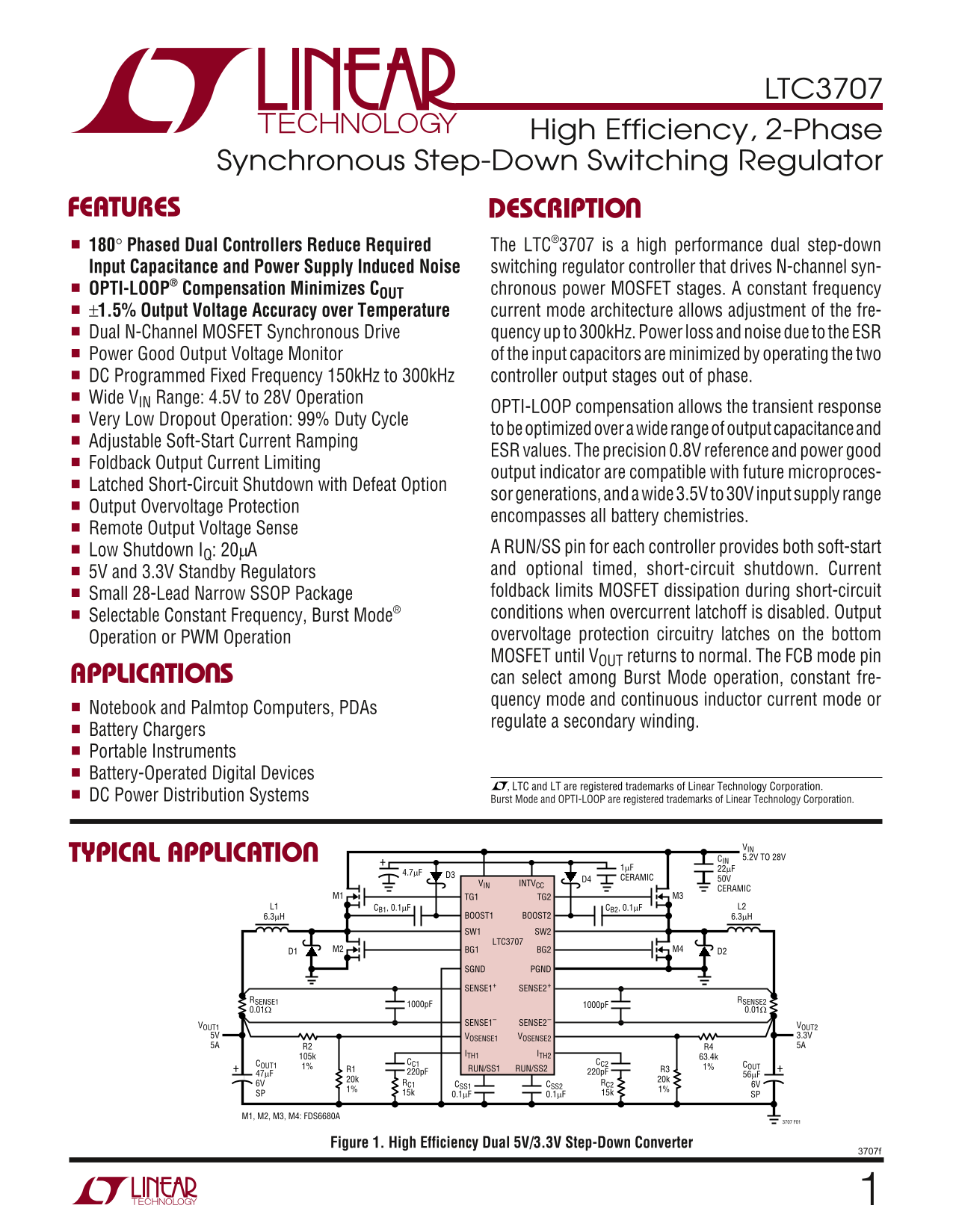
FEATURES DESCRIPTIO 180° Phased Dual Controllers Reduce Required The LTC®3707 is a high performance dual step-down Input Capacitance and Power Supply Induced Noise switching regulator controller that drives N-channel syn- OPTI-LOOP® Compensation Minimizes COUT chronous power MOSFET stages. A constant frequency ±1.5% Output Voltage Accuracy over Temperature current mode architecture allows adjustment of the fre- Dual N-Channel MOSFET Synchronous Drive quency up to 300k Hz. Power loss and noise due to the ESR

Power Good Output Voltage Monitor of the input capacitors are minimized by operating the two DC Programmed Fixed Frequency 150k Hz to 300k Hz controller output stages out of phase.

Wide VIN Range: 4.5V to 28V Operation

OPTI-LOOP compensation allows the transient response

Very Low Dropout Operation: 99% Duty Cycle

to be optimized over a wide range of output capacitance and

Adjustable Soft-Start Current Ramping

ESR values. The precision 0.8V reference and power good

Foldback Output Current Limiting

output indicator are compatible with future microproces-

Latched Short-Circuit Shutdown with Defeat Option

sor generations, and a wide 3.5V to 30V input supply range

Output Overvoltage Protection

encompasses all battery chemistries.

Remote Output Voltage Sense

Low Shutdown IQ: 20µA A RUN/SS pin for each controller provides both soft-start 5V and 3.3V Standby Regulators and optional timed, short-circuit shutdown. Current Small 28-Lead Narrow SSOP Package foldback limits MOSFET dissipation during short-circuit Selectable Constant Frequency, Burst Mode® conditions when overcurrent latchoff is disabled. Output Operation or PWM Operation overvoltage protection circuitry latches on the bottom MOSFET until VOUT returns to normal. The FCB mode pin

APPLICATIO S can select among Burst Mode operation, constant fre-

quency mode and continuous inductor current mode or

Notebook and Palmtop Computers, PDAs

regulate a secondary winding.

Battery Chargers Portable Instruments Battery-Operated Digital Devices

, LTC and LT are registered trademarks of Linear Technology Corporation.

DC Power Distribution Systems Burst Mode and OPTI-LOOP are registered trademarks of Linear Technology Corporation.

VIN TYPICAL APPLICATIO CIN 5.2V TO 28V

D4 CERAMIC 50V

VIN INTVCC

CERAMIC

M1 TG1 TG2 M3

L1 CB1, 0.1µF CB2, 0.1µF L2

6.3µH BOOST1 BOOST2 6.3µH

SW1 SW2 LTC3707

D1 M2 BG1 BG2 D2M4

SGND PGND

SENSE1+ SENSE2+

RSENSE1 RSENSE2

VOUT1 SENSE1– SENSE2– VOUT2

5V VOSENSE1 VOSENSE2 3.3V 5A R2 R4 5A

105k ITH1 ITH2

COUT1 CC1 CC2

1% R1 RUN/SS1 RUN/SS2 R3 1% +COUT

6V RC1 CSS1 CSS2 RC2 6V

SP 15k 0.1µF 0.1µF 15k SP

M1, M2, M3, M4: FDS6680A

Figure 1. High Efficiency Dual 5V/3.3V Step-Down Converter

Page Summary Contents For LINEAR TECHNOLOGY LTC3707 Specifications and User Guide

Page 1 LTC3707 High Efficiency, 2-Phase Synchronous Step-Down Switching Regulator FEATURES DESCRIPTIO 180° Phased Dual Controllers Reduce Required The LTC®3707 is a high performance dual step-down Input Capa...
Page 2 LTC3707 ABSOLUTE AXI U RATI GS PACKAGE/ORDER I FOR ATIO (Note 1) Input Supply Voltage (VIN) .........................30V to –0.3V ORDER PART TOP VIEW Top Side Driver Voltages NUMBER RUN/SS1 PGOOD (BOO...
Page 3 LTC3707 ELECTRICAL CHARACTERISTICS The ● denotes the specifications which apply over the full operating temperature range, otherwise specifications are at TA = 25°C. VIN = 15V, VRUN/SS1, 2 = 5V unless...
Page 4 SU PP LY UR RE NT (µ A) EF FI CI EN CY LTC3707 ELECTRICAL CHARACTERISTICS Note 1: Absolute Maximum Ratings are those values beyond which the life Note 5: Dynamic supply current is higher due to the ga...
Page 5 NO RM AL IZ ED (m V) IN TV CC OL TA GE (V OU EN SE LTC3707 TYPICAL PERFOR A CE CHARACTERISTICS Maximum Current Sense Threshold Maximum Current Sense Threshold vs Percent of Nominal Output Internal 5V ...
Page 6 EN SE (m V) LTC3707 TYPICAL PERFOR A CE CHARACTERISTICS Maximum Current Sense Dropout Voltage vs Output Current Threshold vs Temperature (Figure 13) RUN/SS Current vs Temperature VOUT = 5V DR OP OU VO...
Page 7 CU RR EN SE NS IN PU CU RR EN (µ A) LTC3707 TYPICAL PERFOR A CE CHARACTERISTICS UN DE RV OL TA GE OC KO UT (V Current Sense Pin Input Current EXTVCC Switch Resistance Oscillator Frequency vs Temperatu...
Page 8 LTC3707 PI FU CTIO S RUN/SS1, RUN/SS2 (Pins 1, 15): Combination of soft- 3.3VOUT (Pin 10): Output of a linear regulator capable of start, run control inputs and short-circuit detection timers. supplyi...
Page 9 LTC3707 FU CTIO AL DIAGRA INTVCC VIN DUPLICATE FOR SECOND DB BOOST CONTROLLER CHANNEL FREQSET TG CB OUT CIND1 OSCILLATOR CLK2 DET BOT FCB TOP ON SWITCH INTVCC LOGIC PGOOD 0.86V VFB COUT 0.55V VOUT VSE...
Page 10 LTC3707 OPERATIO (Refer to Functional Diagram) Main Control Loop Low Current Operation The LTC3707 uses a constant frequency, current mode The FCB pin is a multifunction pin providing two func- step-d...
Page 11 LTC3707 (Refer to Functional Diagram)OPERATIO Continuous Current (PWM) Operation linear regulators are turned on independent of the state on the RUN/SS pins of the two switching regulator control- Tyi...
Page 12 LTC3707 (Refer to Functional Diagram)OPERATIO circuit is enabled. Even if a short is present and the short- With 2-phase operation, the two channels of the dual- circuit latchoff is not enabled, a saf...
Page 13 LTC3707 (Refer to Functional Diagram)OPERATIO the RMS input current varies for single-phase and 2-phase becomes more critical with 2-phase operation because operation for 3.3V and 5V regulators over a...
Page 14 LTC3707 FR EQ SE PI VO LT AG (V APPLICATIO S I FOR ATIO 2.5 25% of the current limit determined by RSENSE. Lower inductor values (higher ∆IL) will cause this to occur at lower load currents, which can...
Page 15 LTC3707 APPLICATIO S I FOR ATIO EXTVCC Pin Connection). Consequently, logic-level The term (1+δ) is generally given for a MOSFET in the form threshold MOSFETs must be used in most applications. of a n...
Page 16 LTC3707 APPLICATIO S I FOR ATIO Medium voltage (20V to 35V) ceramic, tantalum, OS-CON operating due to the interleaving of current pulses through and switcher-rated electrolytic capacitors can be used...
Page 17 LTC3707 APPLICATIO S I FOR ATIO Manufacturers such as Nichicon, United Chemicon and recommended. Good bypassing is necessary to supply Sanyo can be considered for high performance through- the high tr...
Page 18 LTC3707 APPLICATIO S I FOR ATIO derived from the output during normal operation (4.7V < 4. EXTVCC Connected to an Output-Derived Boost Net- VOUT < 7V) and from the internal regulator when the ou...
Page 19 LTC3707 APPLICATIO S I FOR ATIO Output Voltage Soft-Start/Run Function The LTC3707 output voltages are each set by an external The RUN/SS1 and RUN/SS2 pins are multipurpose pins feedback resistive div...
Page 20 LTC3707 APPLICATIO S I FOR ATIO Fault Conditions: Overcurrent Latchoff The value of the soft-start capacitor CSS may need to be scaled with output voltage, output capacitance and load The RUN/SS pins ...
Page 21 LTC3707 APPLICATIO S I FOR ATIO Fault Conditions: Overvoltage Protection (Crowbar) provide power to keep-alive functions such as a keyboard controller. This pin can also be used as a latching “on” and...
Page 22 LTC3707 APPLICATIO S I FOR ATIO FCB Pin Operation internal current source pulling the pin high. Include this current when choosing resistor values R5 and R6. The FCB pin can be used to regulate a seco...
Page 23 LTC3707 APPLICATIO S I FOR ATIO Efficiency Considerations 3. I2R losses are predicted from the DC resistances of the fuse (if used), MOSFET, inductor, current sense resistor, The percent efficiency of...
Page 24 LTC3707 APPLICATIO S I FOR ATIO Checking Transient Response full-load current having a rise time of 1µs to 10µs will produce output voltage and ITH pin waveforms that will The regulator loop response ...
Page 25 LTC3707 APPLICATIO S I FOR ATIO Automotive Considerations: Plugging into the just what it says, while double-battery is a consequence of Cigarette Lighter tow-truck operators finding that a 24V jump s...
Page 26 LTC3707 APPLICATIO S I FOR ATIO Design Example Choosing 1% resistors; R1 = 25.5k and R2 = 32.4k yields an output voltage of 1.816V. As a design example for one channel, assume VIN = 12V(nominal), VIN ...
Page 27 LTC3707 APPLICATIO S I FOR ATIO PC Board Layout Checklist 2. Are the signal and power grounds kept separate? The combined LTC3707 signal ground pin and the ground When laying out the printed circuit b...
Page 28 LTC3707 APPLICATIO S I FOR ATIO L1SW1 RSENSE1 VOUT1 COUT1 RL1D1 RIN CIN L2SW2 RSENSE2 VOUT2 COUT2 RL2D2BOLD LINES INDICATE HIGH, SWITCHING CURRENT LINES. KEEP LINES TO A MINIMUM LENGTH. Figure 11. Bra...
Page 29 LTC3707 APPLICATIO S I FOR ATIO 7. Use a modified “star ground” technique: a low imped- Short-circuit testing can be performed to verify proper ance, large copper area central grounding point on the o...
Page 30 LTC3707 TYPICAL APPLICATIO 59k 1M 100k MBRS1100T3 VPULL-UP RUN/SS1 PGOOD PGOOD 0.1µF 0.015Ω VOUT1 SENSE1+ TG1 5V 3A; 4A PEAK 105k, 1% SENSE1– SW1 LT1121 ON/OFF VOSENSE1 BOOST1 220k VOUT3 INTVCC FREQSE...
Page 31 LTC3707 PACKAGE DESCRIPTIO GN Package 28-Lead Plastic SSOP (Narrow .150 Inch) (Reference LTC DWG # 05-08-1641) (9.804 – 9.982) 0.033 (0.838) REF 0° – 8° TYP0.0075 – 0.0098 DIMENSION DOES NOT INCLUDE M...
Page 32 LTC3707 TYPICAL APPLICATIO VPULL-UP (<7V) RUN/SS1 PGOOD PGOOD L1 8µH 0.1µF 0.015Ω VOUT1 SENSE1+ TG1 5V 27p F 1000p F 3A; 4A PEAK 1% SENSE1– SW1 VOSENSE1 BOOST1 INTVCC FREQSET VIN STBYMD BG1 47µF 6....

Manual Details

Brand Linear
Pages 32
File Size 470.11 KB
Published July 22, 2026
0 views

Enter the captcha to get the download link:

captcha

Frequently Asked Questions

What is the acceptable input voltage range for this device?

The LTC3707 operates over a wide supply range of 4.5V to 28V.

What operating modes can I select for the output?

You can select among Burst Mode operation, constant frequency mode, or continuous inductor current mode.

Does it offer protection against abnormal conditions?

Yes, it includes Overvoltage Protection and Latched Short-Circuit Shutdown with a defeat option.

What is the operational temperature range of the regulator?

The device has an operating temperature range specified from -40°C to 85°C.