# A B C D E F G H I J K L M N O P Q R S T U V W X Y Z

LINEAR TECHNOLOGY LT3470 Specifications and User Guide

Summary

The LT3470 is a high-efficiency micropower step-down DC/DC converter designed for demanding battery and industrial power applications. Featuring an integrated boost function, wide input range (4V to 40V), and ultra-low quiescent current, it ensures reliable performance in portable devices and regulated systems. The manual provides detailed specifications on its advanced operational modes, including Burst Mode and protective features, allowing engineers to maintain stable output voltage with minimal size using compact thin packages.
📄 Preview PAGE OF 20

Page 1 Text Content

LT3470

POW ER LOSS (m

Micropower Buck Regulator with Integrated Boost and

Catch Diodes

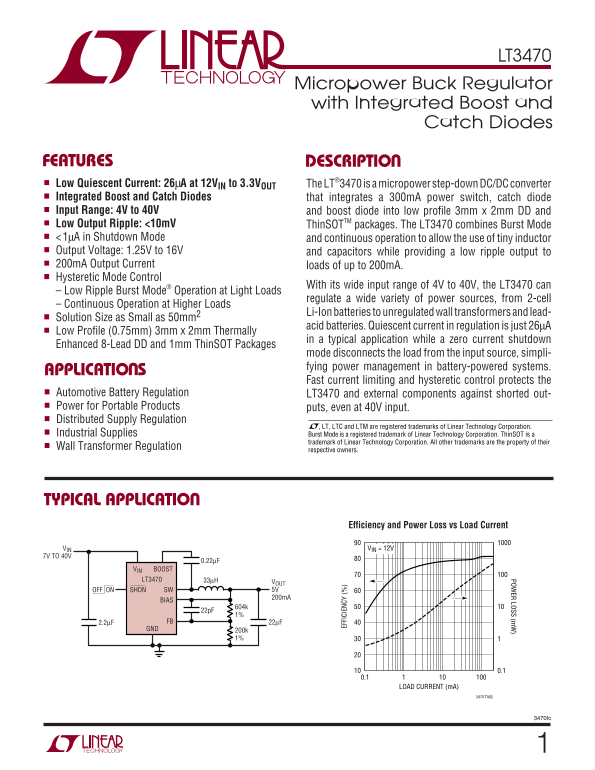
FEATURES DESCRIPTIO Low Quiescent Current: 26µA at 12VIN to 3.3VOUT The LT®3470 is a micropower step-down DC/DC converter Integrated Boost and Catch Diodes that integrates a 300m A power switch, catch diode Input Range: 4V to 40V and boost diode into low profile 3mm x 2mm DD and Low Output Ripple: <10m V Thin SOTTM packages. The LT3470 combines Burst Mode <1µA in Shutdown Mode and continuous operation to allow the use of tiny inductor Output Voltage: 1.25V to 16V and capacitors while providing a low ripple output to 200m A Output Current loads of up to 200m A. Hysteretic Mode Control

With its wide input range of 4V to 40V, the LT3470 can

– Low Ripple Burst Mode® Operation at Light Loads

regulate a wide variety of power sources, from 2-cell

– Continuous Operation at Higher Loads

Li-Ion batteries to unregulated wall transformers and lead-

Solution Size as Small as 50mm2

acid batteries. Quiescent current in regulation is just 26µA

Low Profile (0.75mm) 3mm x 2mm Thermally

in a typical application while a zero current shutdown

Enhanced 8-Lead DD and 1mm Thin SOT Packages EF FI CI EN CY

mode disconnects the load from the input source, simpli- fying power management in battery-powered systems.

APPLICATIO S

Fast current limiting and hysteretic control protects the

Automotive Battery Regulation LT3470 and external components against shorted out- Power for Portable Products puts, even at 40V input. Distributed Supply Regulation

, LT, LTC and LTM are registered trademarks of Linear Technology Corporation.

Industrial Supplies Burst Mode is a registered trademark of Linear Technology Corporation. Thin SOT is a

trademark of Linear Technology Corporation. All other trademarks are the property of their

Wall Transformer Regulation

respective owners.

TYPICAL APPLICATIO

Efficiency and Power Loss vs Load Current

VIN VIN = 12V

7V TO 40V

VIN BOOST LT3470 33µH

VOUT OFF ON SWSHDN 5V 200m A

FB 22µF2.2µF GND 200k

LOAD CURRENT (m A)

3470 TA02

3470fc

Page Summary Contents For LINEAR TECHNOLOGY LT3470 Specifications and User Guide

Page 1 LT3470 POW ER LOSS (m Micropower Buck Regulator with Integrated Boost and Catch Diodes FEATURES DESCRIPTIO Low Quiescent Current: 26µA at 12VIN to 3.3VOUT The LT®3470 is a micropower step-down DC/DC c...
Page 2 LT3470 ABSOLUTE AXI U RATI GS (Note 1) VIN, SHDN Voltage 40V LT3470H 150°C BOOST Pin Voltage 47V Operating Temperature Range (Note 2) BOOST Pin Above SW Pin 25V LT3470E –40°C to 85°C FB Voltage 5V LT3...
Page 3 LT3470 ELECTRICAL CHARACTERISTICS The ● denotes specifications which apply over the full operating temperature range, otherwise specifications are TA = 25°C. VIN = 10V, VSHDN = 10V, VBOOST = 15V, VBIA...
Page 4 CU RR EN LI IT (m A) FI CI EN CY LT3470 TYPICAL PERFOR A CE CHARACTERISTICS SH DN UR RE NT (µ A) Efficiency, VOUT = 5VEfficiency, VOUT = 3.3V VFB vs Temperature L = TOKO D52LC 47µH L = TOKO D52LC 47µH...
Page 5 SC HO TT KY (V FB UR RE NT (µ A) LT3470 TYPICAL PERFOR A CE CHARACTERISTICS FB Bias Current (VFB = 0V) BO OS PI CU RR EN (m A) Switch VCESAT (ISW = 100m A) Boost Diode VF (IF = 50m A) vs Temperature v...
Page 6 SC HO TT KY (V LT3470 TYPICAL PERFOR A CE CHARACTERISTICS Boost Diode Forward Voltage Minimum Input Voltage, VOUT = 3.3V Minimum Input Voltage, VOUT = 5V 6.0 TA = 25°C TA = 25°C VIN TO START VIN TO ST...
Page 7 LT3470 BLOCK DIAGRA VIN BIAS VIN C1 BOOST 500ns ONE SHOT ENABLE BURST MODE DETECT VREF 1.25V FB GND 3470 BD 3470fc
Page 8 LT3470 OPERATIO The LT3470 uses a hysteretic control scheme in conjunc- comparator trips and resets the latch causing the switch to tion with Burst Mode operation to provide low output turn off. While...
Page 9 LT3470 APPLICATIO S I FOR ATIO Input Voltage Range where VIN(MAX) is the maximum input voltage for the application, t ON-TIME(MIN) is ~150ns and IMAX is the maxi- The minimum input voltage required to...
Page 10 LT3470 APPLICATIO S I FOR ATIO Table 2. Inductor Vendors VENDOR URL PART SERIES INDUCTANCE RANGE (µH) SIZE (mm) Coilcraft www.coilcraft.com DO1605 10 to 47 1.8 × 5.4 × 4.2 ME3220 10 to 47 2.0 × 3.2 × ...
Page 11 LT3470 APPLICATIO S I FOR ATIO Ceramic Capacitors BOOST and BIAS Pin Considerations Ceramic capacitors are small, robust and have very low Capacitor C3 and the internal boost Schottky diode (see ESR. ...
Page 12 LT3470 IN PU VO LT AG (V IN PU VO LT AG (V APPLICATIO S I FOR ATIO (Figure 2b). The circuit in Figure 2a is more efficient minimum VIN to start and to run. At light loads, the because the BOOST pin cu...
Page 13 LT3470 APPLICATIO S I FOR ATIO PCB Layout location, ideally at the ground terminal of the output capacitor C2. Additionally, the SW and BOOST nodes For proper operation and minimum EMI, care must be s...
Page 14 LT3470 APPLICATIO S I FOR ATIO Hot-Plugging Safely the voltage overshoot (it also reduces the peak input current). A 0.1µF capacitor improves high frequency filter- The small size, robustness and low ...
Page 15 LT3470 APPLICATIO S I FOR ATIO CLOSING SWITCH SIMULATES HOT PLUG IIN VIN LT3470 VIN 10V/DIV IIN 10A/DIV LOW STRAY IMPEDANCE INDUCTANCE 10µs/DIV ENERGIZED DUE TO 6 FEET 24V SUPPLY (2 METERS) OF TWISTED...
Page 16 LT3470 TYPICAL APPLICATIO S 3.3V Step-Down Converter 5.5V TO 40V C3 0.22µF, 6.3V VIN BOOST LT3470 33µH VOUT OFF ON SWSHDN 3.3V 200m A GND R2 3470 TA03 C1: TDK C3216JB1H105M C2: CE JMK316 BJ226ML-T L1:...
Page 17 LT3470 TYPICAL APPLICATIO S 1.8V Step-Down Converter 4V TO 23V C3 0.22µF, 25V VIN BOOST LT3470 22µH VOUT OFF ON SWSHDN 1.8V 200m A BIAS R1 GND R2 332k 3470 TA05 C1: TDK C3216JB1H105M C2: TDK C2012JB0J...
Page 18 LT3470 PACKAGE DESCRIPTIO TS8 Package 8-Lead Plastic TSOT-23 (Reference LTC DWG # 05-08-1637) 2.90 BSC (NOTE 4) MAX REF 1.22 REF 2.80 BSC 3.85 MAX 1.4 MIN2.62 REF (NOTE 4) PIN ONE ID RECOMMENDED SOLDE...
Page 19 LT3470 PACKAGE DESCRIPTIO DDB Package 8-Lead Plastic DFN (3mm × 2mm) (Reference LTC DWG # 05-08-1702 Rev B) (2 SIDES) TYPR = 0.05 (2 SIDES) 1.15 ±0.05 PIN 1 BAR PIN 1 (2 SIDES) TOP MARK R = 0.20 OR (S...
Page 20 LT3470 RELATED PARTS PART NUMBER DESCRIPTION COMMENTS LT1616 25V, 500m A (IOUT), 1.4MHz, High Efficiency VIN = 3.6V to 25V, VOUT = 1.25V, IQ = 1.9m A, ISD = &lt;1µA, Step-Down DC/DC Converter Thin SOT...

Manual Details

Brand Linear
Pages 20
File Size 256.53 KB
Published June 17, 2026
8 views

Enter the captcha to get the download link:

captcha

Frequently Asked Questions

What is the operating input voltage range for the LT3470?

The device accepts an input range from 4V up to 40V.

How does the LT3470 function in low power states?

It features a shutdown mode with deeply reduced current, achieving less than 1µA draw.

What types of electrical sources can this regulator manage?

It regulates a wide variety of power sources, including Li-Ion batteries and unregulated wall transformers.

Is the device protected against overcurrent issues?

Yes, it includes fast current limiting and hysteretic control to protect components from shorted circuits.