LINEAR TECHNOLOGY LTC3401 Specifications User Guide
Summary
The LTC3401 is a high-efficiency, micropower synchronous boost converter designed for step-up DC/DC voltage regulation in battery-powered devices. Offering up to 97% efficiency and operating across a wide input range (0.5V to 5.5V), it features very low quiescent current and programmable switching frequencies up to 3MHz, which maximizes portable application battery life. This manual details the electrical specifications, operation modes (including Burst Mode), and usage guidelines for implementing stable power solutions in cordless phones, wireless handsets, and backup systems requiring highly reliable, efficient conversion down to sub-2.6V output voltages.
Page 1 Text Content
LTC3401
1A, 3MHz Micropower Synchronous Boost Converter
FEATURES DESCRIPTIO Synchronous Rectification: Up to 97% Efficiency The LTC®3401 is a high efficiency, fixed frequency, step- 1A Switch Current Rating up DC/DC converter that operates from an input voltage
Fixed Frequency Operation Up to 3MHz below 1V. The device includes a 0.16Ω N-channel MOSFET Wide Input Range: 0.5V to 5.5V (Operating) switch and a 0.18Ω P-channel synchronous rectifier. Very Low Quiescent Current: 38µA (Burst Mode® Switching frequencies up to 3MHz are programmed with Operation) an external timing resistor and the oscillator can be 2.6V to 5.5V Adjustable Output Voltage synchronized to an external clock. An external Schottky 0.85V (Typ) Start-Up Voltage diode is optional but will slightly improve efficiency.
No External Schottky Diode Required (VOUT < 4.3V)
Quiescent current is only 38µA in Burst Mode operation,
Synchronizable Switching Frequency
maximizing battery life in portable applications. Burst
Burst Mode Enable Control
Mode operation is user controlled and can be enabled by
Antiringing Control Reduces Switching Noise
driving the MODE/SYNC pin high. If the MODE/SYNC pin
PGOOD Output
has either a clock or is driven low, then fixed frequency
OPTI-LOOP® Compensation
switching is enabled.
Very Low Shutdown Current: <1µA
EF FI CI EN CY Other features include 1µA shutdown, antiringing control,
Small 10-Pin MSOP Package
open-drain power good output, thermal shutdown and
APPLICATIO S current limit. The LTC3401 is available in the 10-lead
thermally enhanced MSOP package. Higher current appli-
Pagers
cations should use the 2A rated LTC3402 synchronous
Handheld Instruments
boost converter. Applications that require VOUT < 2.6V
Cordless Phones
should use the LTC3423.
Wireless Handsets
, LTC and LT are registered trademarks of Linear Technology Corporation.
GPS Receivers Burst Mode and OPTI-LOOP are registered trademarks of Linear Technology Corporation. Battery Backup CCFL Backlights
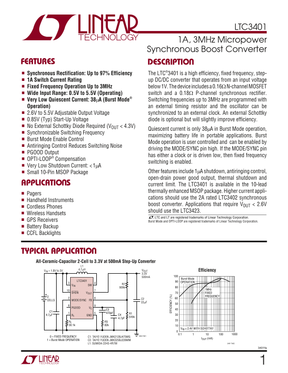
TYPICAL APPLICATION All-Ceramic-Capacitor 2-Cell to 3.3V at 500m A Step-Up Converter
L1 4.7µH VOUT
VIN = 1.8V to 3V Efficiency
Burst Mode
LTC3401
OPERATION
VIN SW
SHDN VOUT FIXED
FREQUENCY
CELLS MODE/SYNC FB
PGOOD VC
4.7µF Rt GND C4 549k 4.7p F
Rt R5 30.1k 82k
VIN = 2.4V WITH SCHOTTKY
0 = FIXED FREQUENCY 3404 TA01
C1: TAIYO YUDEN JMK212BJ475MG
IOUT (m A)
1 = Burst Mode OPERATION C2: TAIYO YUDEN JMK325BJ226MM
L1: SUMIDA CD43-4R7M 3401 TA02
3401fa
Page Summary Contents For LINEAR TECHNOLOGY LTC3401 Specifications User Guide
Manual Details
| Brand | Linear |
|---|---|
| Pages | 16 |
| File Size | 240.71 KB |
| Published | May 31, 2026 |
Enter the captcha to get the download link:

Frequently Asked Questions
What is the operating input voltage range for this converter?
The device operates from a wide input voltage range of 0.5V to 5.5V.
How low can the quiescent current get when in Burst Mode?
In Burst Mode operation, the quiescent current is only 38mA.
What are the different options for synchronizing the switching frequency?
The switching frequency can be synchronized using an external clock and/or controlled via the MODE/SYNC pin.
Which LTC part should be used if the application requires a voltage output below 2.6V?
Applications requiring V<2.6V OUT should use the LTC3423 boost converter.