LINEAR TECHNOLOGY LT3023 Specifications and User Guide
Summary
The LT3023 is a dual, micropower regulator engineered for high-efficiency power management in battery-powered and portable electronics. It delivers ultra-low noise stability (< 20μV) with minimal quiescent current (down to < 0.1μA), ensuring reliable operation across wide input voltage ranges (1.8V to 20V). This technical documentation provides comprehensive specifications, detailed application examples, and electrical characteristics required for integrating this high-performance low dropout regulator into sensitive electronic designs.
Page 1 Text Content
LT3023 Dual 100m A,
Low Dropout, Low Noise, Micropower Regulator
FEATURES DESCRIPTION n Low Noise: 20μVRMS (10Hz to 100k Hz)
The LT®3023 is a dual, micropower, low noise, low drop-
n Low Quiescent Current: 20μA/Channel
out regulator. With an external 0.01μF bypass capacitor,
n Wide Input Voltage Range: 1.8V to 20V
output noise drops to 20μVRMS over a 10Hz to 100k Hz
n Output Current: 100m A/Channel
bandwidth. Designed for use in battery-powered systems,
n Very Low Shutdown Current: <0.1μA
the low 20μA quiescent current per channel makes it an
n Low Dropout Voltage: 300m V at 100m A
ideal choice. In shutdown, quiescent current drops to less
n Adjustable Output from 1.22V to 20V
than 0.1μA. Shutdown control is independent for each
n Stable with 1μF Output Capacitor
channel, allowing for fl exibility in power management. The
n Stable with Aluminum, Tantalum or
device is capable of operating over an input voltage from
Ceramic Capacitors 1.8V to 20V, and can supply 100m A of output current from n Reverse Battery Protected
each channel with a dropout voltage of 300m V. Quiescent
n No Reverse Current
current is well controlled in dropout.
n No Protection Diodes Needed
The LT3023 regulator is stable with output capacitors as
n Overcurrent and Overtemperature Protected
low as 1μF. Small ceramic capacitors can be used without
n Thermally Enhanced 10-Lead MSOP and DFN
the series resistance required by other regulators.
Packages
Internal protection circuitry includes reverse battery APPLICATIONS protection, current limiting, thermal limiting and reverse current protection. The device is available as an adjust-
n Cellular Phones
able device with a 1.22V reference voltage. The LT3023
n Pagers
regulator is available in the thermally enhanced 10-lead
n Battery-Powered Systems
MSOP and DFN packages.
n Frequency Synthesizers
L, LT, LTC and LTM are registered trademarks of Linear Technology Corporation. All other n Wireless Modems trademarks are the property of their respective owners.
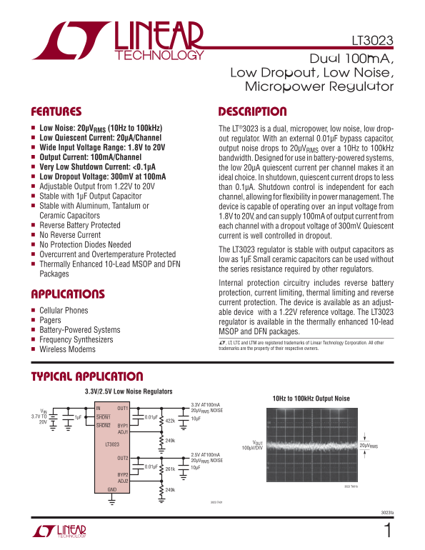
TYPICAL APPLICATION
3.3V/2.5V Low Noise Regulators
10Hz to 100k Hz Output Noise
3.3V AT100m A
IN OUT1
VIN 20μVRMS NOISE
3.7V TO 1μF SHDN1 0.01μF
SHDN2 BYP1
LT3023 20μVRMS
100μV/DIV
2.5V AT100m A
20μVRMS NOISE
BYP2 ADJ2
3023 TA01b
GND 249k
3023 TA01
3023fa
Page Summary Contents For LINEAR TECHNOLOGY LT3023 Specifications and User Guide
Manual Details
| Brand | Linear |
|---|---|
| Pages | 16 |
| File Size | 282.65 KB |
| Published | June 19, 2026 |
Enter the captcha to get the download link:

Frequently Asked Questions
What is the operating temperature range?
The device can operate over an input voltage from –40°C to 125°C.
Does it offer reverse battery protection?
Yes, the internal circuitry includes reverse battery protection.
What is the typical output noise level?
It maintains a low noise of 20μV (10Hz to 100kHz) RMS.
How much current can one channel supply at 3.3V?
One per-channel can supply up to 100mA of output current.