# A B C D E F G H I J K L M N O P Q R S T U V W X Y Z

LINEAR LT3023 Data Sheet

Summary

This dual micropower regulator is engineered for high-efficiency, low-noise power management in battery-powered portable electronics. Featuring 100mA per channel and ultra-low quiescent current (<0.1mA), it ensures stable, clean voltage output across a wide input range (1.8V to 20V). The accompanying manual details critical electrical characteristics, robust protection features (including reverse battery defense), and application guidelines, making the LT3023 the ideal solution for designers creating cellular phones, pagers, and advanced frequency synthesizers.
📄 Preview PAGE OF 16

Page 1 Text Content

查询LT3023供应商

LT3023 Dual 100m A,

Low Dropout, Low Noise, Micropower Regulator

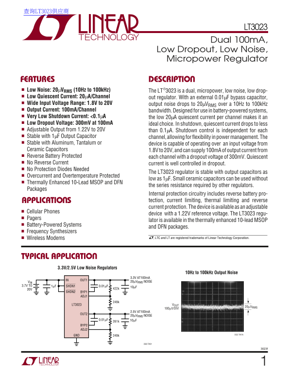
FEATURES DESCRIPTIO Low Noise: 20µVRMS (10Hz to 100k Hz) The LT®3023 is a dual, micropower, low noise, low drop- Low Quiescent Current: 20µA/Channel out regulator. With an external 0.01µF bypass capacitor, Wide Input Voltage Range: 1.8V to 20V output noise drops to 20µVRMS over a 10Hz to 100k Hz Output Current: 100m A/Channel bandwidth. Designed for use in battery-powered systems, Very Low Shutdown Current: <0.1µA the low 20µA quiescent current per channel makes it an Low Dropout Voltage: 300m V at 100m A ideal choice. In shutdown, quiescent current drops to less Adjustable Output from 1.22V to 20V than 0.1µA. Shutdown control is independent for each Stable with 1µF Output Capacitor channel, allowing for flexibility in power management. The Stable with Aluminum, Tantalum or device is capable of operating over an input voltage from Ceramic Capacitors 1.8V to 20V, and can supply 100m A of output current from Reverse Battery Protected each channel with a dropout voltage of 300m V. Quiescent No Reverse Current current is well controlled in dropout. No Protection Diodes Needed

The LT3023 regulator is stable with output capacitors as

Overcurrent and Overtemperature Protected

low as 1µF. Small ceramic capacitors can be used without

Thermally Enhanced 10-Lead MSOP and DFN

the series resistance required by other regulators.

Packages

Internal protection circuitry includes reverse battery pro- APPLICATIO S tection, current limiting, thermal limiting and reverse current protection. The device is available as an adjustable

Cellular Phones

device with a 1.22V reference voltage. The LT3023 regu-

Pagers

lator is available in the thermally enhanced 10-lead MSOP

Battery-Powered Systems

and DFN packages.

Frequency Synthesizers

Wireless Modems , LTC and LT are registered trademarks of Linear Technology Corporation.

TYPICAL APPLICATIO

3.3V/2.5V Low Noise Regulators

10Hz to 100k Hz Output Noise

3.3V AT100m A

IN OUT1VIN

20µVRMS NOISE

3.7V TO 1µF SHDN1 0.01µF

SHDN2 BYP1

LT3023 VOUT

20µVRMS

100µV/DIV

2.5V AT100m A

20µVRMS NOISE

BYP2 ADJ2

3023 TA01b

GND 249k

3023 TA01

Page Summary Contents For LINEAR LT3023 Data Sheet

Page 1 查询LT3023供应商 LT3023 Dual 100m A, Low Dropout, Low Noise, Micropower Regulator FEATURES DESCRIPTIO Low Noise: 20µVRMS (10Hz to 100k Hz) The LT®3023 is a dual, micropower, low noise, low drop- Low Quiesc...
Page 2 LT3023 ABSOLUTE AXI U RATI GS (Note 1) IN Pin Voltage ±20V Output Short-Circut Duration Indefinite OUT1, OUT2 Pin Voltage ±20V Operating Junction Temperature Range Input to Output Differential Voltage...
Page 3 LT3023 ELECTRICAL CHARACTERISTICS The ● denotes specifications which apply over the full operating temperature range, otherwise specifications are TA = 25°C. (Note 2) PARAMETER CONDITIONS MIN TYP MAX ...
Page 4 GN PI CU RR EN (m A) QU IE SC EN CU RR EN (µ A) DR OP OU VO LT AG (m V) LT3023 TYPICAL PERFOR A CE CHARACTERISTICS Typical Dropout Voltage Guaranteed Dropout Voltage Dropout Voltage = TEST POINTS TJ =...
Page 5 RE VE RS OU TP UT UR RE NT (µ A) AD PI BI AS UR RE NT (n A) SH DN IN HR ES HO LD (V LT3023 TYPICAL PERFOR A CE CHARACTERISTICS SHDN1 or SHDN2 Pin Threshold SHDN1 or SHDN2 Pin Input SHDN1 or SHDN2 Pin ...
Page 6 OU TP UT OI SE PE CT RA DE NS IT (µ V/ √H z) CH AN NE L- TO -C HA NN EL IS OL AT IO (d B) RI PP LE EJ EC TI ON (d B) LT3023 TYPICAL PERFOR A CE CHARACTERISTICS Input Ripple Rejection Input Ripple Reje...
Page 7 OU TP UT OI SE (µ S) LT3023 TYPICAL PERFOR A CE CHARACTERISTICS LO AD UR RE NT TP UT OL TA GE (m A) DE VI AT IO (V RMS Output Noise vs 10Hz to 100k Hz Output Noise 10Hz to 100k Hz Output Noise Load Cu...
Page 8 LT3023 PI FU CTIO S GND (Pin 3): Ground. SHDN1/SHDN2 (Pins 7/9): Shutdown. The SHDN1/SHDN2 pins are used to put the corresponding channel of the ADJ1/ADJ2 (Pins 4/2): Adjust Pin. These are the inputs ...
Page 9 LT3023 APPLICATIO S I FOR ATIO The LT3023 is a dual 100m A low dropout regulator with IN OUT1/OUT2 VOUT micropower quiescent current and shutdown. The device VIN OUT ADJ R2LT3023   is capable of s...
Page 10 LT3023 ES (Ω APPLICATIO S I FOR ATIO Output Capacitance and Transient Response dielectrics used are Z5U, Y5V, X5R and X7R. The Z5U and Y5V dielectrics are good for providing high capacitances The LT30...
Page 11 LT3023 APPLICATIO S I FOR ATIO Voltage and temperature coefficients are not the only dissipation from both channels must be considered dur- sources of problems. Some ceramic capacitors have a ing ther...
Page 12 LT3023 APPLICATIONS INFORMATION Calculating Junction Temperature limiting and thermal limiting, the devices are protected against reverse input voltages, reverse output voltages Example: Given an outp...
Page 13 LT3023 APPLICATIO S I FOR ATIO In circuits where a backup battery is required, several TA = 25°C VIN = 0V different input/output conditions can occur. The output VOUT = VADJ voltage may be held up whi...
Page 14 LT3023 PACKAGE DESCRIPTIO DD Package 10-Lead Plastic DFN (3mm × 3mm) (Reference LTC DWG # 05-08-1699) (2 SIDES)2.15 ±0.05 PACKAGE OUTLINE 0.50 BSC 2.38 ±0.05 (2 SIDES) RECOMMENDED SOLDER PAD PITCH AND...
Page 15 LT3023 PACKAGE DESCRIPTIO MSE Package 10-Lead Plastic MSOP (Reference LTC DWG # 05-08-1663) BOTTOM VIEW OF EXPOSED PAD OPTION TYP BSC (NOTE 3) RECOMMENDED SOLDER PAD LAYOUT (NOTE 4) DETAIL “A” 0° – 6°...
Page 16 LT3023 TYPICAL APPLICATIO S Startup Sequencing Turn-On Waveforms VSHDN1 1V/DIV 3.7V TO 20V VOUT1 IN OUT1 AT 1V/DIV LT3023 0.01µF 10µF VOUT2 1µF 1V/DIV BYP1 422k 35.7k 3023 TA03b 2.5V 2ms/DIV OFF ON SH...

Manual Details

Brand Linear
Pages 16
File Size 598.36 KB
Published June 17, 2026
6 views

Enter the captcha to get the download link:

captcha

Frequently Asked Questions

What is the LT3023's output noise level?

The typical output noise is 20mV (10Hz to 100kHz) RMS.

Can I use the LT3023 in battery-powered systems?

Yes, its low quiescent current and design features make it ideal for battery-powered applications.

What voltage range can the device handle?

The input voltage range is wide, spanning from 1.8V to 20V.

How much output current can one channel supply?

Each channel can supply up to 100mA of output current.