# A B C D E F G H I J K L M N O P Q R S T U V W X Y Z

LINEAR LTC1562 Data Sheet

Summary

The LTC1562 is a powerful, low-noise continuous-time active RC quad universal filter, perfect for advanced signal processing and data communications applications. This guide details its functionality as an industry-leading, highly accurate filtering solution. Users can program unique responses—including Butterworth, Chebyshev, and elliptic profiles—across various frequencies (10kHz to 150kHz range) with options for single or dual supply voltages and ultra-high resolution systems. It provides flexible, rail-to-rail input/output, making it ideal for engineers designing precision antialiasing, reconstruction filters, or tunable equalization circuits.
📄 Preview PAGE OF 28

Page 1 Text Content

查询LTC1562供应商

LTC1562

Very Low Noise, Low Distortion Active RC Quad Universal Filter

FEATURES DESCRIPTION

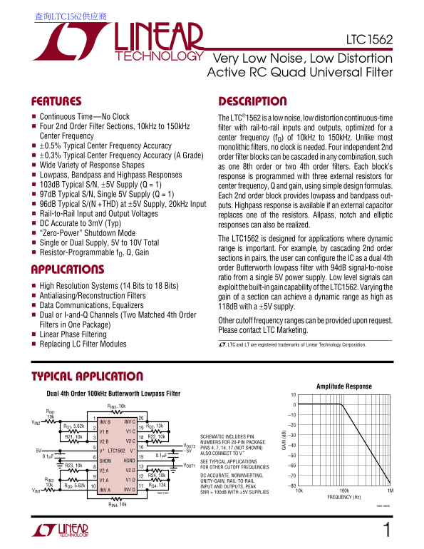
Continuous Time—No Clock The LTC®1562 is a low noise, low distortion continuous-time Four 2nd Order Filter Sections, 10k Hz to 150k Hz filter with rail-to-rail inputs and outputs, optimized for a Center Frequency center frequency (f O) of 10k Hz to 150k Hz. Unlike most ±0.5% Typical Center Frequency Accuracy monolithic filters, no clock is needed. Four independent 2nd ±0.3% Typical Center Frequency Accuracy (A Grade) order filter blocks can be cascaded in any combination, such Wide Variety of Response Shapes as one 8th order or two 4th order filters. Each block’s Lowpass, Bandpass and Highpass Responses response is programmed with three external resistors for 103d B Typical S/N, ±5V Supply (Q = 1) center frequency, Q and gain, using simple design formulas. 97d B Typical S/N, Single 5V Supply (Q = 1) Each 2nd order block provides lowpass and bandpass out- 96d B Typical S/(N + THD) at ±5V Supply, 20k Hz Input puts. Highpass response is available if an external capacitor Rail-to-Rail Input and Output Voltages replaces one of the resistors. Allpass, notch and elliptic DC Accurate to 3m V (Typ) responses can also be realized. “Zero-Power” Shutdown Mode

The LTC1562 is designed for applications where dynamic

Single or Dual Supply, 5V to 10V Total

range is important. For example, by cascading 2nd order

Resistor-Programmable f O, Q, Gain

sections in pairs, the user can configure the IC as a dual 4th APPLICATIONS order Butterworth lowpass filter with 94d B signal-to-noise ratio from a single 5V power supply. Low level signals can

GA IN (d B)

High Resolution Systems (14 Bits to 18 Bits) exploit the built-in gain capability of the LTC1562. Varying the Antialiasing/Reconstruction Filters gain of a section can achieve a dynamic range as high as Data Communications, Equalizers 118d B with a ±5V supply. Dual or I-and-Q Channels (Two Matched 4th Order

Other cutoff frequency ranges can be provided upon request.

Filters in One Package)

Please contact LTC Marketing.

Linear Phase Filtering

Replacing LC Filter Modules , LTC and LT are registered trademarks of Linear Technology Corporation.

TYPICAL APPLICATION

Amplitude Response

Dual 4th Order 100k Hz Butterworth Lowpass Filter

RIN2, 10k

VIN2 INV B INV C

RQ1, 5.62k RQ2, 13k –20

R21, 10k SCHEMATIC INCLUDES PIN

V2 B V2 C NUMBERS FOR 20-PIN PACKAGE.

VOUT2 –40 PINS 4, 7, 14, 17 (NOT SHOWN)

V+ LTC1562 V– –5V5V

ALSO CONNECT TO V–

SHDN AGND SEE TYPICAL APPLICATIONS

R23, 10k VOUT1 –60 FOR OTHER CUTOFF FREQUENCIES

R24, 10k DC ACCURATE, NONINVERTING, –70

RIN3 V1 A V1 D

UNITY-GAIN, RAIL-TO-RAIL

10k RQ3, 5.62k RQ4, 13k –80

INPUT AND OUTPUTS. PEAK

VIN1 INV A INV D 10k 100k 1M

1562 TA01 SNR ≈ 100d B WITH ±5V SUPPLIES

FREQUENCY (Hz)

RIN4, 10k 1562 TA03b

Page Summary Contents For LINEAR LTC1562 Data Sheet

Page 1 查询LTC1562供应商 LTC1562 Very Low Noise, Low Distortion Active RC Quad Universal Filter FEATURES DESCRIPTION Continuous Time—No Clock The LTC®1562 is a low noise, low distortion continuous-time Four 2nd O...
Page 2 LTC1562 PACKAGE/ORDER INFORMATION ABSOLUTE MAXIMUM RATINGS (Note 1) + to V –) Total Supply Voltage (V 11V TOP VIEW ORDER PART Maximum Input Voltage INV B INV C NUMBER – – 0.3V) ≤ V ≤ (V + + 0.3V) V1 B...
Page 3 RR OR LTC1562 ELECTRICAL CHARACTERISTICS VS = ±5V, outputs unloaded, TA = 25°C, SHDN pin to logic “low”, unless otherwise noted. AC specs are for a single 2nd order section, RIN = R2 = RQ =10k ±0.1%, ...
Page 4 NO IS (µ S) ER RO LTC1562 TYPICAL PERFOR A CE CHARACTERISTICS Peak BP Gain vs Nominal f O Peak BP Gain vs Nominal f O (VS = ±5V) (Figure 3, V1 Output)Q Error vs Nominal f O (VS = ±2.5V) (VS = ±2.5V) (...
Page 5 LTC1562 PIN FUNCTIONS (Figure 1). For single supply operation, the AGND pin Shutdown (SHDN): When the SHDN input goes high or is should be bypassed to the ground plane with at least a open-circuited, ...
Page 6 LTC1562 PIN FUNCTIONS INV A, INV B, INV C, INV D: Each of the INV pins is a virtual- order filter section (see Figure 3 and Applications Informa- ground summing point for the corresponding 2nd order t...
Page 7 LTC1562 APPLICATIONS INFORMATION Functional Description Setting f O and Q The LTC1562 contains four matched, 2nd order, 3-termi- Each of the four 2nd order sections in the LTC1562 can be nal universal...
Page 8 LTC1562 GA IN (V /V APPLICATIONS INFORMATION tolerance (by a factor of 2 incrementally), but it also Basic Lowpass implies that R2 has a wider range than f O. (RQ and RIN also When ZIN of Figure 3 is ...
Page 9 LTC1562 APPLICATIONS INFORMATION at frequency f O, and for Q > 0.707, a gain peak occurs at Parameters ωO = 2πf O and Q are set by R2 and RQ as a frequency below f O, as shown in Figure 4. above. T...
Page 10 LTC1562 APPLICATIONS INFORMATION Because 2nd order sections with Q ≥ 1 have response level inputs require further dynamic range, reducing the peaks near f O, the gain ratio above implies some rules of...
Page 11 LTC1562 APPLICATIONS INFORMATION external component ZIN, usually a resistor or capacitor. A practical limitation of this technique is that the CT capaci- This component must of course be rated to sust...
Page 12 LTC1562 APPLICATIONS INFORMATION This procedure can be iterated, adjusting the value of RT, 3d B frequencies f L and f H are widely separated from this to find convenient values for CINA and CINB sinc...
Page 13 LTC1562 TYPICAL APPLICATIONS (Basic) Quad 3rd Order Butterworth Lowpass Filter, Gain = –1 Amplitude Response VOUT1 VOUT2 RIN1BRIN1A RIN2B RIN2A f–3d B = 100k Hz VIN1 INV B INV C VIN2 RQ1 RQ2 CIN1 CIN2...
Page 14 LTC1562 TYPICAL APPLICATIONS (Basic) Dual 4th Order Lowpass Filters Amplitude Response BUTTERWORTH –3d B = 100k Hz VIN2 INV B INV C RQ1 RQ2 –10 VOUT2 –30 V+ LTC1562 V– –5V5V SHDN AGND VOUT1 RQ3 RQ4 VI...
Page 15 LTC1562 TYPICAL APPLICATIONS (Basic) 8th Order Lowpass Filters Amplitude Response CHEBYSHEV RIN1 f C = 100k Hz VIN INV B INV C RQ1 –10 V+ LTC1562 V– –5V5V –40 SHDN AGND –50 RQ3 RQ4 INV A INV D RIN4 –9...
Page 16 LTC1562 (Basic)TYPICAL APPLICATIONS 8th Order Bandpass Filter, Single 5V Supply, Center Frequency –3d B Bandwidth = Amplitude Response f CENTER = 80k Hz VIN INV B INV C –10 RQ1 RQ2 V2 B V2 C –30 5V LT...
Page 17 LTC1562 (Basic)TYPICAL APPLICATIONS 8th Order Bandpass Filter, Single 5V Supply, Center Frequency –1d B Bandwidth = Amplitude Response f CENTER = 100k Hz VIN INV B INV C RQ2 –10 5V V+ LTC1562 V– –40 S...
Page 18 LTC1562 TYPICAL APPLICATIONS (Basic) 8th Order Bandpass (High Frequency) Filter Center Frequency –3d B Bandwidth = , Gain = 10 10 Amplitude Response f CENTER = 100k Hz VIN INV B INV C RQ1 RQ2 V+ LTC15...
Page 19 LTC1562 (Basic)TYPICAL APPLICATIONS 8th Order Wideband Bandpass Filter f CENTER = 50k Hz, –3d B BW 40k Hz to 60k Hz Amplitude Response RIN2 69.8k CIN1 22p F VIN INV B INV C RQ1 59k RQ2 48.7k –10 V+ V+...
Page 20 LTC1562 APPLICATIONS INFORMATION Notches and Elliptic Responses f N. The two signals then cancel out at frequency f N. The notch depth (the completeness of cancellation) will be The basic (essentially...
Page 21 LTC1562 GA IN (d B) APPLICATIONS INFORMATION Note that the depth of the notch depends on the accuracy Feedforward Notches for f N > f0 of this resistor ratioing. The virtual-ground summing When CIN...
Page 22 LTC1562 APPLICATIONS INFORMATION robust against tolerances in the CIN1 value when f N ap- IN IN2 proaches f0 (for f N/f0 ≤ 1.4, as a rule of thumb) which is attractive in narrow transition-band filter...
Page 23 LTC1562 APPLICATIONS INFORMATION R-C Universal Notches DC Gain A different way to get 180° phase shift for a notch is to use     IN the built-in 90° phase difference between the two Opera- tio...
Page 24 LTC1562 TYPICAL APPLICATIONS (Advanced) 8th Order 50k Hz Lowpass Elliptic Filter with 100d B Stopband Attenuation CIN2 24p F RIN2 37.4k Amplitude Response RIN1 48.7k VIN INVB INVC RQ1 30.1k RQ2 13k V+...
Page 25 LTC1562 GA IN (d B) TYPICAL APPLICATIONS (Advanced) 9th Order 22k Hz Lowpass Elliptic Filter RIN2 249k CIN2 33p F CIN3 27p F RIN1A RIN1B PIN 10 VIN INVB INVC CIN1 RQ1 95.3k RQ2 182k R21 324k R22 226k ...
Page 26 LTC1562 TYPICAL APPLICATIONS (Advanced) Dual 5th Order Lowpass “Elliptic” Filter Amplitude Response RIN1BRIN1A VOUT1 VIN1 INVB INVC f C = 100k Hz RQ1 RQ2 5V V+ LTC1562 –5V SHDN AGND RQ1 RQ2 –80 RIN1BR...
Page 27 LTC1562 Dimensions in inches (millimeters) unless otherwise noted.PACKAGE DESCRIPTION G Package 20-Lead Plastic SSOP (0.209) (LTC DWG # 05-08-1640) BSC 0.002 – 0.008 0.010 – 0.015 (0.25 – 0.38)DIMENSI...
Page 28 LTC1562 TYPICAL APPLICATION Amplitude Response Dual 4th Order 12d B Gaussian Lowpass Filter f C = 64k Hz f C = 32k Hz RIN2 –40 RIN1 f C = 16k Hz VIN2 INV B INV C RQ1 RQ2 VOUT2 5V V+ LTC1562 V– 0.1µF 1...

Manual Details

Brand Linear
Pages 28
File Size 466.58 KB
Published June 01, 2026
73 views

Enter the captcha to get the download link:

captcha

Frequently Asked Questions

What total voltage range can the LTC1562 operate within?

It is designed for applications using a single or dual supply in a total range of 5V to 10V.

How can I customize the filter's frequency, Q factor, and gain?

The center frequency (f), Quality (Q), and Gain are programmed by utilizing external resistors via simple design formulas.

What is the maximum useful dynamic range of the filter section?

When supplied with ±5V, the unit can achieve a high signal-to-noise ratio leading to up to 118dB dynamic range.

Is an external component required for certain filtering modes?

Yes, if you wish to utilize the Highpass response, an external capacitor must be connected.