LINEAR Technology LTC1562-2 Data Sheet
Summary
This active RC Quad Universal Filter is a low noise, high performance component designed for advanced signal conditioning in critical electronics applications. It provides four independent, configurable second-order filter sections—capable of realizing lowpass, bandpass, and highpass responses—without needing an external clock signal. The manual details utilizing its programmable center frequency, Q, and gain across single or dual power supplies, enabling precise filtering for antialiasing, equalizers, and data communication systems. Ideal for engineers designing high-resolution (14-18 bits) and wide bandwidth instrumentation where maintaining signal integrity is paramount.
Page 1 Text Content
查询LTC1562-2供应商
LTC1562-2
Very Low Noise, Low Distortion Active RC Quad Universal Filter
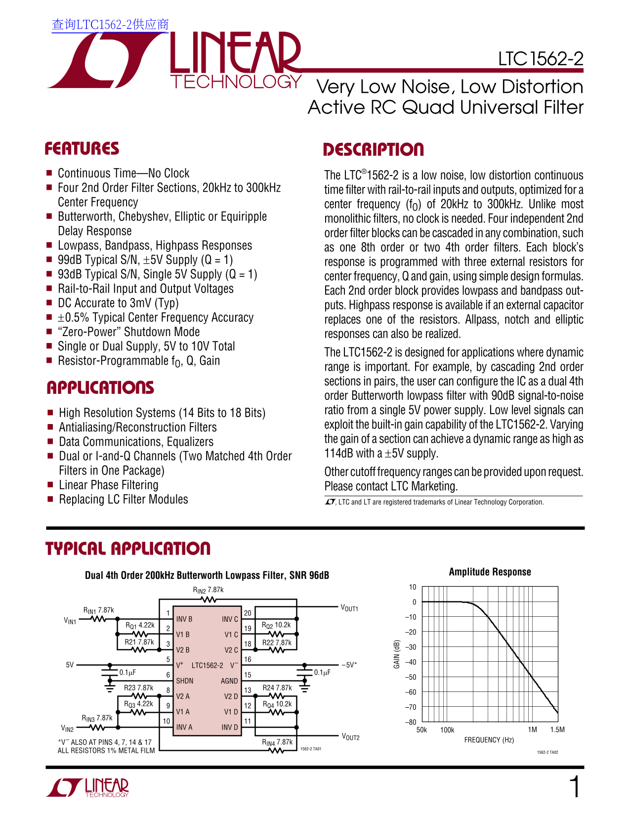
FEATURES DESCRIPTIO Continuous Time—No Clock The LTC®1562-2 is a low noise, low distortion continuous Four 2nd Order Filter Sections, 20k Hz to 300k Hz time filter with rail-to-rail inputs and outputs, optimized for a Center Frequency center frequency (f O) of 20k Hz to 300k Hz. Unlike most Butterworth, Chebyshev, Elliptic or Equiripple monolithic filters, no clock is needed. Four independent 2nd Delay Response order filter blocks can be cascaded in any combination, such Lowpass, Bandpass, Highpass Responses as one 8th order or two 4th order filters. Each block’s 99d B Typical S/N, ±5V Supply (Q = 1) response is programmed with three external resistors for 93d B Typical S/N, Single 5V Supply (Q = 1) center frequency, Q and gain, using simple design formulas. Rail-to-Rail Input and Output Voltages Each 2nd order block provides lowpass and bandpass out- DC Accurate to 3m V (Typ) puts. Highpass response is available if an external capacitor ±0.5% Typical Center Frequency Accuracy replaces one of the resistors. Allpass, notch and elliptic “Zero-Power” Shutdown Mode responses can also be realized. Single or Dual Supply, 5V to 10V Total
The LTC1562-2 is designed for applications where dynamic
Resistor-Programmable f O, Q, Gain
range is important. For example, by cascading 2nd order sections in pairs, the user can configure the IC as a dual 4th
APPLICATIO S
GA IN (d B) order Butterworth lowpass filter with 90d B signal-to-noise
ratio from a single 5V power supply. Low level signals can
High Resolution Systems (14 Bits to 18 Bits)
exploit the built-in gain capability of the LTC1562-2. Varying
Antialiasing/Reconstruction Filters
the gain of a section can achieve a dynamic range as high as
Data Communications, Equalizers
114d B with a ±5V supply.
Dual or I-and-Q Channels (Two Matched 4th Order Filters in One Package) Other cutoff frequency ranges can be provided upon request. Linear Phase Filtering Please contact LTC Marketing. Replacing LC Filter Modules , LTC and LT are registered trademarks of Linear Technology Corporation.
TYPICAL APPLICATIO
Amplitude Response
Dual 4th Order 200k Hz Butterworth Lowpass Filter, SNR 96d B
RIN2 7.87k
VOUT1
RIN1 7.87k
INV B –10
VIN1 INV C
RQ1 4.22k RQ2 10.2k
5V V+ LTC1562-2 V– –5V*
SHDN AGND
RQ3 4.22k RQ4 10.2k
RIN3 7.87k
VIN2 INV A INV D
VOUT2
RIN4 7.87k FREQUENCY (Hz)
*V– ALSO AT PINS 4, 7, 14 & 17
1562-2 TA01
ALL RESISTORS 1% METAL FILM 1562-2 TA02
Page Summary Contents For LINEAR Technology LTC1562-2 Data Sheet
Manual Details
| Brand | Linear |
|---|---|
| Pages | 16 |
| File Size | 183.12 KB |
| Published | July 16, 2026 |
Enter the captcha to get the download link:
