# A B C D E F G H I J K L M N O P Q R S T U V W X Y Z

LINEAR TECHNOLOGY LT1610 Specifications and User Guide

Summary

This comprehensive manual details the LT1610 micropower fixed frequency DC/DC converter, designed for ultra-low power applications. It provides critical electrical characteristics, operational guidelines, and sample circuits for efficiently boosting voltage in miniature portable electronics. Ideal for engineers designing products like pagers, cordless phones, or battery backup systems that require reliable power conversion from low input voltages (down to 1V).
📄 Preview PAGE OF 16

Page 1 Text Content

LT1610

1.7MHz, Single Cell Micropower DC/DC Converter

FEATURES DESCRIPTIO Uses Tiny Capacitors and Inductor The LT®1610 is a micropower fixed frequency DC/DC Internally Compensated converter that operates from an input voltage as low as 1V. Low Quiescent Current: 30µA Intended for small, low power applications, it switches at Operates with VIN as Low as 1V 1.7MHz, allowing the use of tiny capacitors and inductors. 3V at 30m A from a Single Cell

The device can generate 3V at 30m A from a single cell

5V at 200m A from 3.3V

(1V) supply. An internal compensation network can be

High Output Voltage Capability: Up to 28V

connected to the LT1610’s VC pin, eliminating two exter-

Low Shutdown Current: <1µA

nal components. No-load quiescent current of the LT1610

Automatic Burst Mode TM Switching at Light Load

is 30µA, and the internal NPN power switch handles a

Low VCESAT Switch: 300m V at 300m A

300m A current with a voltage drop of 300m V.

8-Lead MSOP and SO Packages

The LT1610 is available in 8-lead MSOP and SO packages.

APPLICATIO S

EF FI CI EN CY

Pagers Cordless Phones Battery Backup LCD Bias

, LTC and LT are registered trademarks of Linear Technology Corporation. Portable Electronic Equipment Burst Mode is a trademark of Linear Technology Corporation.

TYPICAL APPLICATIO

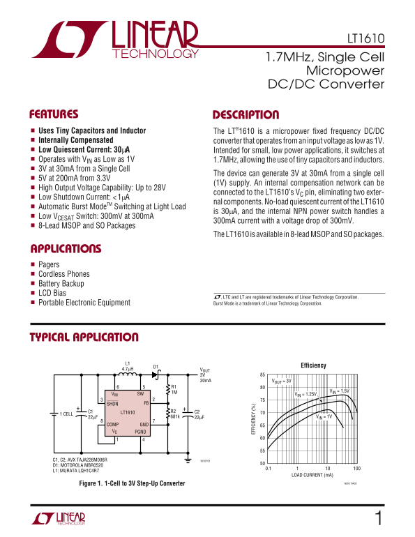
D1 Efficiency

4.7µH VOUT

3V 30m A VOUT = 3V

1M VIN = 1.5V

VIN SW VIN = 1.25V

FBSHDN

LT1610

1 CELL

22µF 681k 22µF VIN = 1V

GNDCOMP

VC PGND

C1, C2: AVX TAJA226M006R 1610 F01 D1: MOTOROLA MBR0520

L1: MURATA LQH1C4R7

LOAD CURRENT (m A)

Figure 1. 1-Cell to 3V Step-Up Converter 1610 TA01

Page Summary Contents For LINEAR TECHNOLOGY LT1610 Specifications and User Guide

Page 1 LT1610 1.7MHz, Single Cell Micropower DC/DC Converter FEATURES DESCRIPTIO Uses Tiny Capacitors and Inductor The LT®1610 is a micropower fixed frequency DC/DC Internally Compensated converter that oper...
Page 2 LT1610 ABSOLUTE MAXIMUM RATINGS (Note 1) VIN Voltage 8V Maximum Junction Temperature 125°C SW Voltage –0.4V to 30V Operating Temperature Range (Note 1) FB Voltage VIN + 0.3V Commercial 0°C to 70°C VC ...
Page 3 LT1610 ELECTRICAL CHARA TERISTICS The ● denotes specifications which apply over the specified temperature range, otherwise specifications are at TA = 25°C. Commercial grade 0°C to 70°C, VIN = 1.5V, VS...
Page 4 SW IT CH IN FR EQ UE NC (M Hz SH DN UR RE NT (µ A) (m V) ES AT LT1610 TYPICAL PERFOR A CE CHARACTERISTICS Current Limit (DC = 30%) vs Temperature Current Limit vs Duty Cycle VCESAT vs Current TA = 25°...
Page 5 LT1610 PIN FUNCTIONS VC (Pin 1): Error Amplifier Output. Frequency compensa- SW (Pin 5): Switch Pin. Connect inductor/diode here. tion network must be connected to this pin, either internal Minimize t...
Page 6 LT1610 APPLICATIONS INFORMATION OPERATION If the output load increases sufficiently, A1’s output remains high, resulting in continuous operation. When the LT1610 The LT1610 combines a current mode, fi...
Page 7 LT1610 APPLICATIONS INFORMATION A SEPIC (Single-Ended Primary Inductance Converter) that spans (i.e., can be higher or lower than) the output. schematic is shown in Figure 4. This converter topology R...
Page 8 LT1610 APPLICATIONS INFORMATION COMPONENT SELECTION impedance of the output capacitor. The capacitor should have low impedance at the 1.7MHz switching frequency of Inductors the LT1610. At this freque...
Page 9 LT1610 APPLICATIONS INFORMATION CERAMIC VOUT 5V 120m A VIN SW L2 C1 C4 VC 22µH 4 CELLS 22µF 1µF LT1610 C2 C5 6.3V CERAMIC 324k 22µF 1µF COMP SHDN 6.3V CERAMIC GND PGND C1, C2: ALUMINUM ELECTROLYTIC C3...
Page 10 LT1610 APPLICATIONS INFORMATION output capacitor because it introduces a zero in the regulator’s loop gain. This zero may not be effective because the ceramic capacitor’s ESR is very low. Most VOUT 10...
Page 11 LT1610 TYPICAL APPLICATIONS Efficiency2-Cell to 5V Converter 4.7µH VOUT VIN = 3V VIN = 2V VIN SW FBSHDN VIN = 1.5V C1 LT1610 C2 2 CELLS 324k GNDCOMP VC PGND C1, C2: AVX TAJA156M010R 1610 TA02 LOAD CUR...
Page 12 LT1610 TYPICAL APPLICATIONS 5V to 9V/150m A Boost Converter Efficiency 10µH VOUT VIN SW FBVC +C1 LT1610 R3 C2 SHDNCOMP GND PGND C1: AVX TAJA156M010 1610 TA08 SHUTDOWN LOAD CURRENT (m A) C2: AVX TAJB15...
Page 13 LT1610 TYPICAL APPLICATIONS 3.3V TO 8V/70m A, –8V/5m A, 24V/5m A TFT LCD Bias Supply Uses All Ceramic Capacitors VOFF –8V 1µF 5m A D3 VON 0.22µF: TAIYO YUDEN EMK212BJ224MG 1µF: TAIYO YUDEN LMK212BJ105...
Page 14 LT1610 OU TP UT UR RE NT (m A) TYPICAL APPLICATIONS Single Cell Super Cap Charger VOUT 4.5V R1 CHARGE 200k VIN SW COMPSHDN C1 LT1610 SHUTDOWN GND PGND 15k1 AA ALKALINE R3 845k 1610 TA11 C1, C2: AVX TA...
Page 15 LT1610 PACKAGE DESCRIPTION Dimensions in inches (millimeters) unless otherwise noted. MS8 Package 8-Lead Plastic MSOP (LTC DWG # 05-08-1660) 0° – 6° TYP SEATING PLANE 0.021 ± 0.006 0.012 0.006 ± 0.004...
Page 16 LT1610 TYPICAL APPLICATIONS N Li-Ion to 3.3V SEPIC DC/DC Converter Efficiency VIN = 2.7V L1 VIN = 3.6V CERAMIC 22µH D1INPUT VOUT VIN = 4.2V Li-ION 3.3V 3V to 4.2V 120m A VIN SW L2 C1 VC 22µH LT1610 C2...

Manual Details

Brand Linear
Pages 16
File Size 214.13 KB
Published June 02, 2026
51 views

Enter the captcha to get the download link:

captcha

Frequently Asked Questions

What is the minimum input voltage for the LT1610 converter?

It operates from an input voltage as low as 1V.

Can this device handle high output voltages?

Yes, it supports a high output voltage capability of up to 28V connected to the V pin.

What is the unit's quiescent/shutdown current?

The standard no-load quiescent current is less than 1mA, and the shutdown current varies between 0.5mA and 1.0mA depending on the mode.

Which packages are available for the LT1610?

It is available in 8-lead MSOP and SO packages.