# A B C D E F G H I J K L M N O P Q R S T U V W X Y Z

LINEAR TECHNOLOGY LTC1876 User's Manual

Summary

The LTC1876 is a high-performance switching controller offering triple regulated outputs, including dual step-down regulators and a boost step-up regulator. Designed for advanced power management, its manual details features like operation over wide voltage ranges (3.5V to 36V), ultra-low dropout capability, and optimized soft-start functions. This versatile chip is ideal for powering modern portable devices, including notebooks, PDAs, and battery-operated electronics that require high efficiency and reliable power delivery.
📄 Preview PAGE OF 36

Page 1 Text Content

LTC1876

High Efficiency, 2-Phase,

Dual Synchronous Step-Down Switching Controller and Step-Up Regulator

FEATURES DESCRIPTIO Step-Down Controller The LTC®1876 is a high performance triple output switching

Out-of-Phase Controllers Reduce Required Input regulator. It incorporates a dual step-down switching con- Capacitance and Power Supply Induced Noise troller that drives all N-channel synchronous power MOSFET Power Good Output Voltage Indicator stages. A step-up regulator with an internal 1A, 36V switch OPTI-LOOPTM Compensation Minimizes COUT provides the third output.

DC Programmed Fixed Frequency 150k Hz to 300k Hz

The step-down controllers minimize power loss and noise

Wide VIN Range: 3.5V to 36V Operation

by operating the output stage of each controller out of

Very Low Dropout Operation: 99% Duty Cycle phase. OPTI-LOOP compensation allows the transient Adjustable Soft-Start Current Ramping response to be optimized over a wide range of output Latched Short-Circuit Shutdown with Defeat Option capacitance and ESR values. A RUN/SS pin for each Remote Output Voltage Sense and OV Protection controller provides both soft-start and an optional timed, 5V and 3.3V Standby Regulators short-circuit shutdown that can be configured to latch off Selectable Const. Freq. or Burst Mode TM Operation one or both controllers. Current foldback provides

Step-Up Regulator additional short-circuit protection. In an overvoltage High Operating Switching Frequency of 1.2MHz condition, the bottom MOSFET is latched on until VOUT Low Internal VCESAT Switch: 400m V @ 1A, VIN = 3V returns to normal. The FCB pin can be used to inhibit Burst Wide VIN Range: 2.6V to 16V Operation Mode operation or to enable regulation of a secondary High Output Voltage: Up to 34V output voltage. The step-up regulator operates at 1.2MHz, allowing the

APPLICATIO S

use of tiny low cost capacitors and inductors. In addition, 3.3V Input Step-Down Converter its internal 1A switch allows high current outputs to be Notebook and Palmtop Computers, PDAs generated. Its current mode control scheme provides Battery-Operated Digital Devices excellent line and load regulation. , LTC and LT are registered trademarks of Linear Technology Corporation. Burst Mode and OPTI-LOOP are trademarks of Linear Technology Corporation.

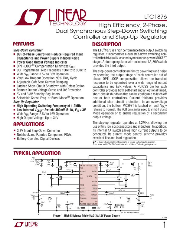
TYPICAL APPLICATIO

VIN 5.2V

TO 28V

35V 1µF VOUT3

CER CER 12V

ALUM 10V

AUXVIN VININTVCC

M3 TG2 TG1 M1 10µF

BOOST2 BOOST1

SW2 SW1

LTC1876 6.8µH

M4 BG2 BG1 M2

AUXSW

PGND AUXVFB

PGOOD AUXSD

SENSE2+ SENSE1+

VOUT2 SENSE2– SENSE1– VOUT1 3.3V 5V

VOSENSE2 VOSENSE1 4A

1% ITH2 ITH1

4V 220p F RUN/SS2 SGND RUN/SS1 220p F 6.3V

SP SP

M1, M2, M3, M4: FDS6680A

1876 TA01

Figure 1. High Efficiency Triple 5V/3.3V/12V Power Supply

1876fa

Page Summary Contents For LINEAR TECHNOLOGY LTC1876 User's Manual

Page 1 LTC1876 High Efficiency, 2-Phase, Dual Synchronous Step-Down Switching Controller and Step-Up Regulator FEATURES DESCRIPTIO Step-Down Controller The LTC®1876 is a high performance triple output switch...
Page 2 LTC1876 ABSOLUTE AXI RATI GS PACKAGE/ORDER I FOR ATIO (Note 1) Input Supply Voltage (VIN) 36V to –0.3V ORDER PART TOP VIEW Topside Driver Voltages NUMBER RUN/SS1 PGOOD (BOOST1, BOOST2) 42V to –0.3V SE...
Page 3 LTC1876 ELECTRICAL CHARACTERISTICS The ● denotes the specifications which apply over the full operating temperature range, otherwise specifications are at TA = 25°C. VIN = 15V, VRUN/SS1, 2 = 5V, AUXVI...
Page 4 LTC1876 ELECTRICAL CHARACTERISTICS The ● denotes the specifications which apply over the full operating temperature range, otherwise specifications are at TA = 25°C. VIN = 15V, VRUN/SS1, 2 = 5V, AUXVI...
Page 5 IN TV CC OL TA GE (V SU PP LY UR RE NT (µ A) EF FI CI EN CY LTC1876 TYPICAL PERFOR A CE CHARACTERISTICS Efficiency vs Output Current and Efficiency vs Output Current Efficiency vs Input Voltage Mode (...
Page 6 EN SE (m V) NO RM AL IZ ED OU EN SE (m V) LTC1876 TYPICAL PERFOR A CE CHARACTERISTICS Maximum Current Sense Maximum Current Sense Threshold vs Sense Common Current Sense Threshold Threshold vs VRUN/SS...
Page 7 FE ED BA CK OL TA GE (V SH UT DO LA TC TH RE SH OL DS (V EX TV IT CH ES IS TA NC (Ω LTC1876 TYPICAL PERFOR A CE CHARACTERISTICS EXTVCC and Switch Resistance vs Oscillator Frequency vs Undervoltage Loc...
Page 8 LTC1876 TYPICAL PERFOR A CE CHARACTERISTICS Input Source/Capacitor Instantaneous Current (Figure 1) Load Step (Figure 1) Load Step (Figure 1) IIN 2A/DIV VOUT VOUT VIN 200m V/DIV 200m V/DIV 200m V/DIV ...
Page 9 LTC1876 PIN FUNCTIONS provides a common control point to shut down both control- TG1, TG2 (Pins 35, 24): High Current Gate Drives for Top lers. See the Operation section for details. N-Channel MOSFETs...
Page 10 LTC1876 FUNCTIONAL DIAGRA INTVCC VIN DUPLICATE FOR SECOND DB BOOST CONTROLLER CHANNEL FREQSET TG CB OUT CIND1 OSCILLATOR CLK2 DET BOT FCB TOP ON PGOOD SWITCH INTVCC LOGIC RUN/SS1 BG WINDOW VOSENSE1 CO...
Page 11 LTC1876 (Refer to Functional Diagram)OPERATIO Main Control Loop AUX Regulator The LTC1876 uses a constant frequency, current mode The auxiliary boost regulator is completely independent scheme to prov...
Page 12 LTC1876 (Refer to Functional Diagram)OPERATIO cycles, followed by a variable “sleep” interval depending This allows the INTVCC power to be derived from a high upon the load current. The resultant outp...
Page 13 LTC1876 (Refer to Functional Diagram)OPERATIO controller has been started and been given adequate time Why the need for 2-phase operation? In most dual con- to charge up the output capacitors and prov...
Page 14 LTC1876 (Refer to Functional Diagram)OPERATIO path, which could include batteries, switches, trace/con- the input capacitor requirement to that for just one channel nector resistances and protection c...
Page 15 LTC1876 APPLICATIO S I FOR ATIO Selection of Operating Frequency operation, lower inductance values will cause the burst frequency to decrease. The LTC1876 uses a constant frequency architecture with ...
Page 16 LTC1876 APPLICATIO S I FOR ATIO then, sub-logic level threshold MOSFETs (VGS(TH) < 3V) The term (1 + δ) is generally given for a MOSFET in the should be used. Pay close attention to the BVDSS speci...
Page 17 LTC1876 APPLICATIO S I FOR ATIO Medium voltage (20V to 35V) ceramic, tantalum, OS-CON controllers are operating due to the reduced overlap of and switcher-rated electrolytic capacitors can be used as ...
Page 18 LTC1876 APPLICATIO S I FOR ATIO discharge during the operating frequency period due to KEMET T510 series of surface mount tantalums, available ripple current. The choice of using smaller output capaci...
Page 19 LTC1876 APPLICATIO S I FOR ATIO operating frequency as discussed in the Efficiency Consid- The following list summarizes the four possible connec- erations section. The junction temperature can be est...
Page 20 LTC1876 APPLICATIO S I FOR ATIO the internal precision 0.8V voltage reference by the error 1µF VIN amplifier. The output voltage is given by the equation: BAT85 0.22µF BAT85 VIN OUT LTC1876 N-CH BAT85...
Page 21 LTC1876 APPLICATIO S I FOR ATIO Soft-Start/Run Function Fault Conditions: Overcurrent Latchoff The RUN/SS1 and RUN/SS2 pins are multipurpose pins The RUN/SS pins also provide the ability to latch off ...
Page 22 LTC1876 APPLICATIO S I FOR ATIO The value of the soft-start capacitor CSS may need to be to protect against a shorted top MOSFET if the short scaled with output voltage, output capacitance and load oc...
Page 23 LTC1876 APPLICATIO S I FOR ATIO approximately 220k Hz. The FREQSET pin can be grounded synchronous switch duty factor. Thus, the FCB input pin to lower this frequency to approximately 140k Hz or tied ...
Page 24 LTC1876 APPLICATIO S I FOR ATIO Voltage Positioning 1. The VIN current has two components: the first is the DC supply current given in the Electrical Characteristics table, Voltage positioning can be ...
Page 25 LTC1876 APPLICATIO S I FOR ATIO quadrupling the importance of loss terms in the switching damping factor can be estimated using the percentage of regulator system! overshoot seen at this pin. The band...
Page 26 LTC1876 APPLICATIO S I FOR ATIO TO SENSE1+ Low VIN Applications INPUT AND SENSE1– SUPPLY In applications where the input supply is low (<5V), the L1 RS1 ITH1 LTC1876 auxiliary regulator can be used...
Page 27 LTC1876 APPLICATIO S I FOR ATIO Once the value of L is known, select an inductor that can between VOUT3 and AUXVFB as shown in Figure 11. The handle at least 1A without saturating. In addition, ensure...
Page 28 LTC1876 APPLICATIO S I FOR ATIO Automotive Considerations: Plugging into the Design Example Cigarette Lighter As a design example for one channel, assume VIN = 12V As battery-powered devices go mobile...
Page 29 LTC1876 APPLICATIO S I FOR ATIO Choosing 1% resistors; R1 = 25.5k and R2 = 32.4k yields Since the required output current is 300m A, the ripple an output voltage of 1.816V. current of the inductor is ...
Page 30 LTC1876 APPLICATIO S I FOR ATIO PC Board Layout Checklist 1. Are the top N-channel MOSFETs M1 and M3 located within 1cm of each other with a common drain connection When laying out the printed circuit...
Page 31 LTC1876 APPLICATIO S I FOR ATIO signal ground pin and the ground return of CINTVCC must the (–) plates of the COUT3 (–) plates by placing the return to the combined COUT (–) plates. Within the regula-...
Page 32 LTC1876 APPLICATIO S I FOR ATIO 6. Are the SENSE– and SENSE+ leads routed together with The duty cycle percentage should be maintained from minimum PC trace spacing? The filter capacitor between cycle...
Page 33 LTC1876 APPLICATIO S I FOR ATIO An embarrassing problem, which can be missed in an will not be realized. Compensation of the voltage loop will otherwise properly working switching regulator, results b...
Page 34 LTC1876 TYPICAL APPLICATIO S 3.3VIN Dual-Phase High Efficiency Power Supply VPULL-UP RUN/SS1 PGOOD L1 0.9µH VOUT1 SENSE1+ TG1 2.5V 17.4k RSENSE SENSE1– SW1 VOSENSE1 BOOST1 1µF FREQSET VIN 0.01µF VIN 3...
Page 35 LTC1876 PACKAGE DESCRIPTIO G Package 36-Lead Plastic SSOP (5.3mm) (Reference LTC DWG # 05-08-1640) 0.42 ±0.03 0.65 BSC RECOMMENDED SOLDER PAD LAYOUT BSC 0.05 NOTE: (.002) (.009 – .015) G36 SSOP 0802 1...
Page 36 LTC1876 TYPICAL APPLICATION High Efficiency Triple 5V/ 3.3V/12V Power Supply VPULL-UP RUN/SS1 PGOOD L1 4.6µH VOUT1 SENSE1+ TG1 3.3V 63.4k RSENSE SENSE1– SW1 VOSENSE1 BOOST1 VIN 47µF FREQSET VIN 6.3V 5...

Manual Details

Brand Linear
Pages 36
File Size 359.56 KB
Published June 21, 2026
9 views

Enter the captcha to get the download link:

captcha

Frequently Asked Questions

What is the primary function of this regulator?

It is a high performance triple output switching regulator that incorporates both dual step-down and one step-up controller functions.

What safety protections does the device offer?

Protection features include latched short-circuit shutdown, Overvoltage Protection (OV), and current foldback for redundancy.

How can I optimize power loss and noise reduction?

OPTI-LOOP compensation minimizes C OUT capacitance and helps minimize overall power loss through phased output stage operation.

What are the usable input voltage specifications?

The device supports a wide operating voltage range, spanning from 3.5V up to 36V.