# A B C D E F G H I J K L M N O P Q R S T U V W X Y Z

LINEAR TECHNOLOGY LTC1873 User's Manual

Summary

The LTC1873 is a high-performance dual switching regulator controller designed for sophisticated, low-voltage power delivery applications. This IC integrates two independent, synchronous 2-Phase PWM regulators on one chip, ensuring maximum efficiency and fast transient response crucial for modern CPUs and I/O core supplies. Featuring Intel Desktop VID compliance (5-Bit voltage adjustment), it maintains stable performance at a fixed 550kHz frequency without relying on external current sense resistors. Ideal for power supply designers creating complex electronics requiring highly regulated, multi-rail power within constrained space and strict efficiency guidelines.
📄 Preview PAGE OF 32

Page 1 Text Content

LTC1873

Dual 550k Hz Synchronous 2-Phase Switching Regulator Controller with 5-Bit VID

FEATURES DESCRIPTIO Two Independent PWM Controllers in One Package The LTC®1873 is a dual switching regulator controller opti- Side 1 Output Is Compliant with Intel Desktop mized for high efficiency with low input voltages. It includes VRM 8.4 Specifications (Includes 5-Bit VID DAC) two complete, on-chip, independent switching regulator con-

1.3V to 3.5V Output Voltage with 50m V/100m V Steps trollers. Each is designed to drive a pair of external Two Sides Run Out-of-Phase to Minimize CIN N-channel MOSFETs in a voltage mode feedback, synchro- All N-Channel External MOSFET Architecture nous buck configuration. The LTC1873 includes digital out- No External Current Sense Resistors Required put voltage adjustment on side 1 that conforms to the Intel Precison Internal 0.8V ±1% Reference Desktop VID specification. A constant-frequency, true PWM 550k Hz Switching Frequency Minimizes External design minimizes external component size and cost and Component Size optimizes load transient performance. The synchronous buck Very Fast Transient Response architecture automatically shifts to discontinuous and then to Up to 25A Output Current per Channel Burst Mode TM operation as the output load decreases, ensur-

Low Shutdown Current: < 100µA ing maximum efficiency over a wide range of load currents. Small 28-Pin SSOP Package

The LTC1873 features an onboard reference trimmed to 1% and delivers better than 1.5% regulation at the converter APPLICATIO S outputs over all combinations of line, load and temperature. Each channel can be enabled independently; with both chan-

Microprocessor Core and I/O Supplies

nels disabled, the LTC1873 shuts down and supply current

Multiple Logic Supply Generator

drops below 100µA.

High Efficiency Power Conversion

, LTC and LT are registered trademarks of Linear Technology Corporation.

Chipset Power Supply Burst Mode is a trademark of Linear Technology Corporation.

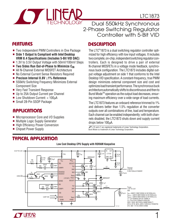
TYPICAL APPLICATIO

Low Cost Desktop CPU Supply with RDRAM Keepalive

4.5V TO 5.5V IN OUT 1µF LT1761

10Ω CIN 16.2k

GND ADJ 0.1%

MBR0530T

VCC PVCC

FB2 BOOST2 16.9k

TG2 QT2 1µF L2

COMP2 VRDRAM SW2 2.5V/7A 2.45V/100m A STANDBY

1k RUN/SS2 BG2 QB2

COUT2

RUN/SS1 47k

0.1µF IMAX2

STBY/ON 1k QSS2

LTC1873 FAULT MBR0530T SENSE BOOST1

QT1B 1µF

220p F TG1 QT1A L1

56k 39p F VCORE COMP1 SW1 1.3V TO 3.5V

BG1 QB1A

FCB COUT1 CIN = SANYO 10MV1200GX (6 IN PARALLEL)

33k COUT1 = SANYO 6MV1500GX (8 IN PARALLEL) 5-BIT VID VID4:0 IMAX1 COUT2 = SANYO 6MV1500GX (3 IN PARALLEL) L1: 1µH SUMIDA CEP125-1R0MC-H

SGND PGND

L2: 2.2µH COILTRONICS UP2B-2R2 QSS1, QSS2: MOTOROLA MMBT3904LT1 QT1A, QT1B, QB1A, QB1B: FAIRCHILD FDS6670A 1873 TA01 QT2, QB2: 1/2 SILICONIX Si4966

Page Summary Contents For LINEAR TECHNOLOGY LTC1873 User's Manual

Page 1 LTC1873 Dual 550k Hz Synchronous 2-Phase Switching Regulator Controller with 5-Bit VID FEATURES DESCRIPTIO Two Independent PWM Controllers in One Package The LTC®1873 is a dual switching regulator con...
Page 2 LTC1873 ABSOLUTE AXI U RATI GS PACKAGE/ORDER I FOR ATIO (Note 1) TOP VIEW ORDER PART Supply Voltage PVCC IMAX2 NUMBER VCC 7V BOOST1 BOOST2 BOOSTn..........................................................
Page 3 LTC1873 ELECTRICAL CHARACTERISTICS The ● denotes specifications which apply over the full operating temperature range, otherwise specifications are TA = 25°C. VCC = 5V unless otherwise specified. (Not...
Page 4 SO UR CE UR RE NT (µ A) SU PP LY UR RE NT (m A) EF FI CI EN CY LTC1873 TYPICAL PERFOR A CE CHARACTERISTICS MOSFET Driver Supply Current Efficiency vs Load Current Transient Response vs Gate Capacitanc...
Page 5 LTC1873 PI FU CTIO S PVCC (Pin 1): Driver Power Supply Input. PVCC provides FCB (Pin 7): Force Continuous Bar. The FCB pin forces power to the two BGn output drivers. PVCC must be both converters to m...
Page 6 LTC1873 PI FU CTIO S VIDn pin includes an on-chip 40kΩ pull-up resistor in disabled. When FAULT is high, both BG pins will go high, series with a diode (see Block Diagram). turning on the bottom MOSFE...
Page 7 LTC1873 BLOCK DIAGRA FCB PVCC VCC BOOST1,2 BURST TG1,2 LOGIC DRIVE SW1,2 LOGIC BG1,2 90% DUTY CYCLE PGND OSC SGND 550k Hz SOFT 10µA RUN/SS1,2 START FAULT UU WU COMP1,2 0V 25µs DELAY 10µA FB MIN MAX FL...
Page 8 LTC1873 APPLICATIO S I FOR ATIO Table 1. VID Inputs and Corresponding Output Voltage for Channel 1 CODE VID4 VID3 VID2 VID1 VID0 VOUT1 CODE VID4 VID3 VID2 VID1 VID0 VOUT1 GND GND GND GND GND 2.05V Flo...
Page 9 LTC1873 APPLICATIO S I FOR ATIO factor of 3.75. The reduced input ripple voltage also means The voltage mode feedback loop and MOSFET VDS current less power is lost in the input power path, which coul...
Page 10 LTC1873 APPLICATIO S I FOR ATIO Switching Architecture frequency band with the 550k Hz frequency designed to leave the 455k Hz IF band free of interference. Subharmonic Each half of the LTC1873 is des...
Page 11 LTC1873 APPLICATIO S I FOR ATIO pin. The output is connected to COMP, which is in turn to resume normal operation when the fault is removed. connected to the soft-start circuitry and from there to the...
Page 12 LTC1873 APPLICATIO S I FOR ATIO Each RUN/SS pin shuts down its half of the LTC1873 when Any time QB is on and the current flowing to the output is it falls below about 0.5V (Figure 4). Between 0.5V an...
Page 13 LTC1873 APPLICATIO S I FOR ATIO enhance loop stability. Larger overloads cause the soft- Selection section for a detailed description of ripple start capacitor to pull down quickly, protecting the out...
Page 14 LTC1873 IN DU CT OR UR RE NT APPLICATIO S I FOR ATIO DU CT OR UR RE NT is most severe, and by including a few millivolts offset in Burst Mode Operation the comparator that monitors the SW node. Despit...
Page 15 LTC1873 APPLICATIO S I FOR ATIO FCB Pin OVERVOLTAGE FAULT In some circumstances, it is desirable to control or disable The LTC1873 includes a single overvoltage fault flag for discontinuous and Burst ...
Page 16 LTC1873 APPLICATIO S I FOR ATIO normal operation. The MAX comparator will act as usual, other hand, voltage breakdown requirements in a typical turning on QB until output is within range and then LTC1...
Page 17 LTC1873 APPLICATIO S I FOR ATIO that it all has to come out of VCC to turn the MOSFET gate INPUT SUPPLY on, and when the MOSFET is turned back off, that charge The Bi CMOS process that allows the LTC1...
Page 18 LTC1873 APPLICATIO S I FOR ATIO maintain the input voltage until the input supply can make Calculating RMS Current in CIN up the difference. Generally, a capacitor that meets the first two parameters ...
Page 19 LTC1873 AC IN PU CU RR EN (A APPLICATIO S I FOR ATIO from CIN (time point A). 50% of the way through, TG2 current and resistive losses, but this approximate value turns on and the total current is 13A...
Page 20 LTC1873 APPLICATIO S I FOR ATIO inductor should be rated to withstand 15A + 1/2 IRIPPLE, OUTPUT BYPASS CAPACITOR or 16.5A without saturating. The output bypass capacitor has quite different require- m...
Page 21 LTC1873 APPLICATIO S I FOR ATIO So far, the AC response of the loop is pretty well out of the user’s control. The modulator is a fundamental piece of the C1 LTC1873 design, and the external L and C ar...
Page 22 LTC1873 APPLICATIO S I FOR ATIO C2 Modulator gain and phase can be measured directly from R3 a breadboard, or can be simulated if the appropriate C1 R2 parasitic values are known. Measurement will giv...
Page 23 LTC1873 APPLICATIO S I FOR ATIO V(OUT) in degrees. Refer to your SPICE manual for details Now calculate the remaining values: of how to generate this plot. (K is a constant used in the calculations) *...
Page 24 LTC1873 APPLICATIO S I FOR ATIO CURRENT LIMIT PROGRAMMING Accuracy Trade-Offs Programming the current limit on the LTC1873 is straight- The VDS sensing scheme used in the LTC1873 is not forward. The I...
Page 25 LTC1873 APPLICATIO S I FOR ATIO with 20m V of hysteresis, allowing fairly precise control of later removed, the LTC1873 will latch off again unless the the auxiliary voltage. If the LTC1873 is in disc...
Page 26 LTC1873 APPLICATIO S I FOR ATIO Maximizing Low Load Current Efficiency pin, which encompasses both reference accuracy and any op amp offset. This accounts for 1% error at the output Low load current e...
Page 27 LTC1873 APPLICATIO S I FOR ATIO TRANSIENT RESPONSE does so (Figure 15). Positive di/dt in the inductor causes positive dv/dt in the ESR, regardless of what the “pure” Transient response is the other h...
Page 28 LTC1873 APPLICATIO S I FOR ATIO VSW VOUT COUT IOUT Figure 15a. Capacitor Parasitics Affecting Transient Recovery IL IOUT VESR VCAP VOUT(NOMINAL) TRANSIENT IL &gt; IOUT TIME HITS VOUT TURNS AROUND Figu...
Page 29 LTC1873 APPLICATIO S I FOR ATIO Implementing voltage positioning is as simple as creating Measurement Techniques an intentional resistance in the output path to generate the Measuring transient respon...
Page 30 LTC1873 APPLICATIO S I FOR ATIO the actual load for the test, and switch it on and off while Changing the Output Voltage on the Fly watching the output. If this isn’t convenient, a current step The vo...
Page 31 LTC1873 PACKAGE DESCRIPTIO Dimensions in inches (millimeters) unless otherwise noted. G Package 28-Lead Plastic SSOP (0.209) (LTC DWG # 05-08-1640) BSC 0.05 – 0.21 (0.010 – 0.015)NOTE: DIMENSIONS ARE ...
Page 32 LTC1873 TYPICAL APPLICATIO Single Output, 2-Phase, 25A VID Converter (VIN = 5V, VOUT = 1.3V to 3.5V) VIN 5V LT®1218 470µF* MBR0530T 470µF* MBR VCC PVCC 330p F SENSE FB1 BOOST1 COMP1 TG1 Q1 1µH 47k VOU...

Manual Details

Brand Linear
Pages 32
File Size 314.14 KB
Published June 18, 2026
1 views

Enter the captcha to get the download link:

captcha

Frequently Asked Questions

What is the maximum output current per channel?

The device can provide up to 25A Output Current per Channel.

Does the LTC1873 require external resistors for sensing?

No External Current Sense Resistors Required, simplifying the design.

What kind of multiple supplies does this chip support?

It is designed for Microprocessor Core and I/O Supplies (e.g., desktop CPU supply).

What is the operating temperature range for the LTC1873?

The operational temperature range is specified as –40°C to 85°C.