# A B C D E F G H I J K L M N O P Q R S T U V W X Y Z

LINEAR TECHNOLOGY LTC1702 User's Manual

Summary

This synchronous 2-phase switching regulator controller is designed for high-efficiency power management in dual-output applications requiring stable core and I/O supplies. Optimized for low input voltages, it features two independent controllers operating out-of-phase through a constant-frequency 550kHz PWM design. The accompanying manual details its advanced synchronous buck architecture, which minimizes external components while ensuring exceptional output regulation (as low as 1%). Ideal for systems needing superior efficiency across wide load ranges and integrated fault protection logic.
📄 Preview PAGE OF 36

Page 1 Text Content

LTC1702

Dual 550k Hz Synchronous

2-Phase Switching Regulator Controller

FEATURES DESCRIPTIO

Two Independent Controllers in One Package The LTC®1702 is a dual switching regulator controller opti- Two Sides Run Out-of-Phase to Minimize CIN mized for high efficiency with low input voltages. It includes All N-Channel External MOSFET Architecture two complete, on-chip, independent switching regulator No External Current Sense Resistors controllers each designed to drive a pair of external N-channel Excellent Output Regulation: 1% Total Output MOSFET devices in a voltage mode feedback, synchronous Accuracy buck configuration. The LTC1702 uses a constant-frequency, 550k Hz Switching Frequency Minimizes External true PWM design switching at 550k Hz, minimizing external Component Size component size and cost and maximizing load transient 1A to 25A Output Current per Channel performance. The synchronous buck architecture automati- High Efficiency over Wide Load Current Range cally shifts to discontinuous and then to Burst Mode TM Quiescent Current Drops Below 100µA in Shutdown operation as the output load decreases, ensuring maximum Small 24-Pin Narrow SSOP Package efficiency over a wide range of load currents. The LTC1702 features an onboard reference trimmed to

APPLICATIO S 0.5% and can provide better than 1% regulation at the

converter outputs. Open-drain logic outputs indicate whether

Microprocessor Core and I/O Supplies

either output has risen to within 5% of the final output voltage

Multiple Logic Supply Generator

and an optional latching FAULT mode protects the load if the

Distributed Power Applications

output rises 15% above the intended voltage. Each channel

High Efficiency Power Conversion

can be enabled independently; with both channels disabled, the LTC1702 shuts down and supply current drops below

, LTC and LT are registered trademarks of Linear Technology Corporation. Burst Mode is a trademark of Linear Technology Corporation. 100µA.

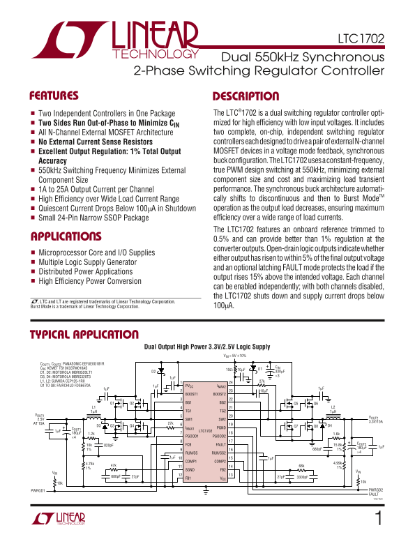
TYPICAL APPLICATIO

Dual Output High Power 3.3V/2.5V Logic Supply

VIN = 5V ±10%

COUT1, COUT2: PANASONIC EEFUE0G181R

CIN: KEMET TS10X337M010AS CIN

D1, D2: MOTOROLA MBR0520LT1 D2 330µF D3, D4: MOTOROLA MBRS320T3 ×3

L1, L2: SUMIDA CEP125-1R0 27k Q1 TO Q8: FAIRCHILD FDS6670A 1µF PVCC IMAX2

BOOST1 BOOST2

Q2Q1 BG1 BG2 Q5 Q6

1µH TG1 TG2 1µH

VOUT1

VOUT2

2.5V SW1 SW2

AT 15A 27k

COUT1 IMAX1 PGND 1µF LTC1702

×4 PGOOD1 PGOOD2

FCB FAULT COUT2

RUN/SS RUN/SS2 ×4

COMP1 COMP2

SGND FB2

VIN VIN

FB1 VCC

PWRGD1 PWRGD2 FAULT 1702 TA01

Page Summary Contents For LINEAR TECHNOLOGY LTC1702 User's Manual

Page 1 LTC1702 Dual 550k Hz Synchronous 2-Phase Switching Regulator Controller FEATURES DESCRIPTIO Two Independent Controllers in One Package The LTC®1702 is a dual switching regulator controller opti- Two S...
Page 2 LTC1702 ABSOLUTE MAXIMUM RATINGS PACKAGE/ORDER INFORMATION (Note 1) TOP VIEW ORDER PART Supply Voltage PVCC IMAX2 NUMBER1 VCC 7V BOOST1 BOOST2 BOOSTn......................................................
Page 3 LTC1702 ELECTRICAL CHARACTERISTICS The ● denotes specifications which apply over the full operating temperature range, otherwise specifications are TA = 25°C. VCC = 5V unless otherwise specified. (Not...
Page 4 SO UR CE UR RE NT (µ A) SU PP LY UR RE NT (m A) EF FI CI EN CY LTC1702 TYPICAL PERFOR A CE CHARACTERISTICS MOSFET Driver Supply Current Efficiency vs Load Current Transient Response vs Gate Capacitanc...
Page 5 LTC1702 PIN FUNCTIONS PVCC (Pin 1): Driver Power Supply Input. PVCC provides FB1 falls 5% below its programmed value. When RUN/SS1 power to the two BGn output drivers. PVCC must be is low (side 1 shut...
Page 6 LTC1702 PIN FUNCTIONS FB2 (Pin 14): Controller 2 Feedback Input. See FB1. disable latched FAULT mode and will allow the LTC1702 to resume normal operation when the overvoltage fault is COMP2 (Pin 15):...
Page 7 LTC1702 TEST CIRCUIT Test Circuit 1 IBOOST1 ICC IPVCC IBOOST2 VCC PVCC BOOST1 BOOST2 f OSC TG1 TG2 MEASURED BG1 BG2 SW1 SW2 CL CL CL CL 5V 10k IMAX1 IMAX2 LTC1702 10k VPGOOD1 PGOOD1 PGOOD2 VPGOOD2 FAU...
Page 8 LTC1702 APPLICATIONS INFORMATION 2-Step Conversion regulation system happens in the 5V supply, which is usually located away from the CPU. The power lost to heat “2-step” architectures use a primary r...
Page 9 LTC1702 APPLICATIONS INFORMATION 2, remember that the power losses are proportional to IRMS High Efficiency meaning that the actual power wasted is reduced by a The LTC1702 uses a synchronous step-dow...
Page 10 LTC1702 APPLICATIONS INFORMATION amp of continuous current with peak currents up to 5A to tion with a simple external charge pump (Figure 2), this slew large MOSFET gates quickly. The external MOSFETs...
Page 11 LTC1702 APPLICATIONS INFORMATION improves loop phase margin (see Figure 3). The Feedback Notice that the FB pin is the virtual ground node of the Loop/Compensation section contains a detailed explana-...
Page 12 LTC1702 APPLICATIONS INFORMATION SHUTDOWN/SOFT-START 10%. The maximum duty cycle limit increases linearly between 1V and 2.5V, reaching its final value of 90% when Each half of the LTC1702 has a RUN/S...
Page 13 LTC1702 APPLICATIONS INFORMATION Any time QB is on and the current flowing to the output is DISCONTINUOUS/Burst Mode OPERATION reasonably large, the SW node at the drain of QB will be Theory of operat...
Page 14 LTC1702 IN DU CT OR UR RE NT DU CT OR UR RE NT APPLICATIONS INFORMATION ripple voltage and frequency remain constant at all loads, on. Since QB acts like a resistor, SW should ideally be right easing ...
Page 15 LTC1702 APPLICATIONS INFORMATION Once again, the LTC1702 switches to a new mode to Paralleling Outputs minimize efficiency loss: Burst Mode operation. As the Synchronous regulators (like the LTC1702) ...
Page 16 LTC1702 APPLICATIONS INFORMATION FAULT mode is used, a Schottky diode should be added is 3.3V) to minimize resistive power loss while they are with its cathode at the output and its anode at ground to...
Page 17 LTC1702 APPLICATIONS INFORMATION charge, actual parasitic drain-source capacitance and MOSFET(s). For very large external MOSFETs (or multiple Miller-multiplied gate-drain capacitance, but can be ap- ...
Page 18 LTC1702 APPLICATIONS INFORMATION must be low enough to keep the initial drop as QT turns on Calculating RMS Current in CIN within reason (100m V or so); its RMS current capability must be adequate to ...
Page 19 LTC1702 AC IN PU CU RR EN (A APPLICATIONS INFORMATION from CIN (time point A). 50% of the way through, TG2 turns on and the total current is 13A (time point B). Shortly thereafter, TG1 turns off and t...
Page 20 LTC1702 APPLICATIONS INFORMATION tantalum capacitors specifically designed for use with ON OUT switching regulators. When choosing a tantalum input RIPPLE capacitor, make sure that it is rated to carr...
Page 21 LTC1702 APPLICATIONS INFORMATION feedback amplifier, on the other hand, gives us a handle configuration is stable but transient response will be less with which to adjust the AC response. The goal is ...
Page 22 LTC1702 APPLICATIONS INFORMATION “Type 3” loops (Figure 11) use two poles and two zeros to Applications that require optimized transient response will obtain a 180° phase boost in the middle of the fr...
Page 23 LTC1702 APPLICATIONS INFORMATION nodes don’t corrupt the measurements or damage the Finally, choose a convenient resistor value for R1 (10k is analyzer. usually a good value). Now calculate the remain...
Page 24 LTC1702 APPLICATIONS INFORMATION CURRENT LIMIT PROGRAMMING Accuracy Trade-Offs Programming the current limit on the LTC1702 is straight- The VDS sensing scheme used in the LTC1702 is not forward. The ...
Page 25 LTC1702 APPLICATIONS INFORMATION VIN The FAULT pin is an additional open-drain output that VOUT(AUX) indicates if one or both of the outputs has exceeded 15% CIN of its programmed output voltage. FAUL...
Page 26 LTC1702 APPLICATIONS INFORMATION to an intermediate supply voltage, often 5V. The LTC1702 Clearly, the 5V and 3.3V sections of the two schemes are then converts the intermediate voltage to the low vol...
Page 27 LTC1702 APPLICATIONS INFORMATION 2-Step Efficiency Calculation Maximizing High Load Current Efficiency Calculating the efficiency of a 2-step converter system Efficiency at high load currents (when th...
Page 28 LTC1702 APPLICATIONS INFORMATION Maximizing Low Load Current Efficiency offset. This accounts for 1% error at the output with a 5V input supply. The feedback voltage line regulation spec Low load curr...
Page 29 LTC1702 APPLICATIONS INFORMATION cycles. Over just a few cycles, however, the external Note that the output voltage will stop dropping before the components conspire to limit the speed that the output...
Page 30 LTC1702 APPLICATIONS INFORMATION Making L smaller than this optimum value yields little or no Optimizing Loop Compensation improvement in transient response. As the output voltage Loop compensation ha...
Page 31 LTC1702 APPLICATIONS INFORMATION it goes out of spec. Similarly, at full load, the output current oscilloscope turned on to limit high frequency noise. Note can only decrease, causing a positive shift...
Page 32 LTC1702 APPLICATIONS INFORMATION FAULT BEHAVIOR never programmed to step down by more than 15% in any single step. The safest strategy is to step the output down Changing the Output Voltage on the Fly...
Page 33 LTC1702 TYPICAL APPLICATIONS ua l O ut pu t P ow er up pl BR 0µ PV CC BO OS T1 BO OS T2 XT P1 P2 1µ 1µ 1µ XT Q1 TG TG Q1 UT UT 1. 8V SW SW 3. 3V Q2 BG LT C1 BG Q2 D2 BR 0T1µ 7k R1 C3 AX 2, C3 0. 1% 0p...
Page 34 LTC1702 TYPICAL APPLICATIONS Si ng le ut pu t, 2- Ph as e, in im um ap ac ito rs to .5 V/ Co nv er te D3 N1 , C OU T, VC C: UR AT GR 5Y 5V 6Z N2 : A VX PS D1 0R D1 , D 2, 3: OT OR OL BR T1 AL OS FE TS...
Page 35 LTC1702 PACKAGE DESCRIPTION Dimensions in inches (millimeters) unless otherwise noted. GN Package 24-Lead Plastic SSOP (Narrow 0.150) (LTC DWG # 05-08-1641) (0.838) REF 0° – 8° TYP0.007 – 0.0098 DIMEN...
Page 36 LTC1702 TYPICAL APPLICATION Low Cost Dual Supply with 2.5V Keepalive 5V IN OUT 1µF LT1761 10Ω CIN 16.2k GND ADJ 0.1% MBR0530T VCC PVCC FB2 BOOST2 16.9k TG2 QT2 1µF L2 VOUT2 COMP2 RUN/SS2 BG2 QB2 STAND...

Manual Details

Brand Linear
Pages 36
File Size 357.25 KB
Published June 16, 2026
2 views

Enter the captcha to get the download link:

captcha

Frequently Asked Questions

What is the switching frequency used by the LTC1702 regulator?

It uses a constant-frequency, accuracy PWM design that switches at 550kHz.

How does the device protect the load from overvoltage conditions?

An optional latching FAULT mode protects the load if the output voltage rises 15% above the intended value.

What is the quiescent current draw when the regulator is shut down?

When both channels are independently disabled, the supply current drops below 100mA and the unit shuts down.

What level of regulation accuracy can be achieved at the converter outputs?

The onboard reference allows the LTC1702 to provide better than 1% regulation at the converter outputs.