# A B C D E F G H I J K L M N O P Q R S T U V W X Y Z

LINEAR TECHNOLOGY LTC1530 User's Manual

Summary

This comprehensive guide details the LTC1530, a high-power synchronous switching regulator controller designed for mission-critical power applications. Ideal for engineers developing industrial and commercial hardware that requires reliable, efficient voltage conversion from 5V or 3.3V down to 1.3V–3.5V. The manual covers key features like top-side FET sensing (eliminating external resistors), adjustable current limiting, and over 95% peak efficiency. It provides deep technical specifications necessary for integrating stable, high-performance power solutions into microprocessors and embedded systems.
📄 Preview PAGE OF 24

Page 1 Text Content

LTC1530

High Power Synchronous Switching Regulator Controller

FEATURES DESCRIPTIO High Power Buck Converter from 5V or 3.3V Input The LTC®1530 is a high power synchronous switching Adjustable Current Limit in S0-8 with regulator controller optimized for 5V to 1.3V-3.5V output Topside FET RDS(ON) Sensing applications. Its synchronous switching architecture drives No External Sense Resistor Required two external N-channel MOSFET devices to provide high Hiccup Mode Current Limit Protection efficiency. The LTC1530 contains a precision trimmed Adjustable, Fixed 1.9V, 2.5V, 2.8V and 3.3V Output reference and feedback system that provides worst-case All N-Channel MOSFET Synchronous Driver output voltage regulation of ±2% over temperature, load Excellent Output Regulation: ±2% over Line, Load current and line voltage shifts. Current limit circuitry and Temperature Variations senses the output current through the on-resistance of High Efficiency: Over 95% Possible the topside N-channel MOSFET, providing an adjustable Fast Transient Response current limit without requiring an external low value sense Fixed 300k Hz Frequency Operation resistor. Internal Soft-Start Circuit

The LTC1530 includes a fixed frequency PWM oscillator

Quiescent Current: 1m A; 45µA in Shutdown

that free runs at 300k Hz, providing greater than 90% efficiency in converter designs from 1A to 20A of output APPLICATIO S current. Shutdown mode drops the LTC1530 supply cur-

EF FI CI EN CY

rent to 45µA.

Power Supply for Pentium® II, AMD-K6®-2, SPARC,

The LTC1530 is specified for commercial and industrial

ALPHA and PA-RISC Microprocessors

temperature ranges and is available in the S0-8 package.

High Power 5V to 1.3V-3.5V Regulators

, LTC and LT are registered trademarks of Linear Technology Corporation. Pentium is a registered trademark of Intel Corp. AMD-K6 is a registered trademark of Advanced Micro Devices, Inc.

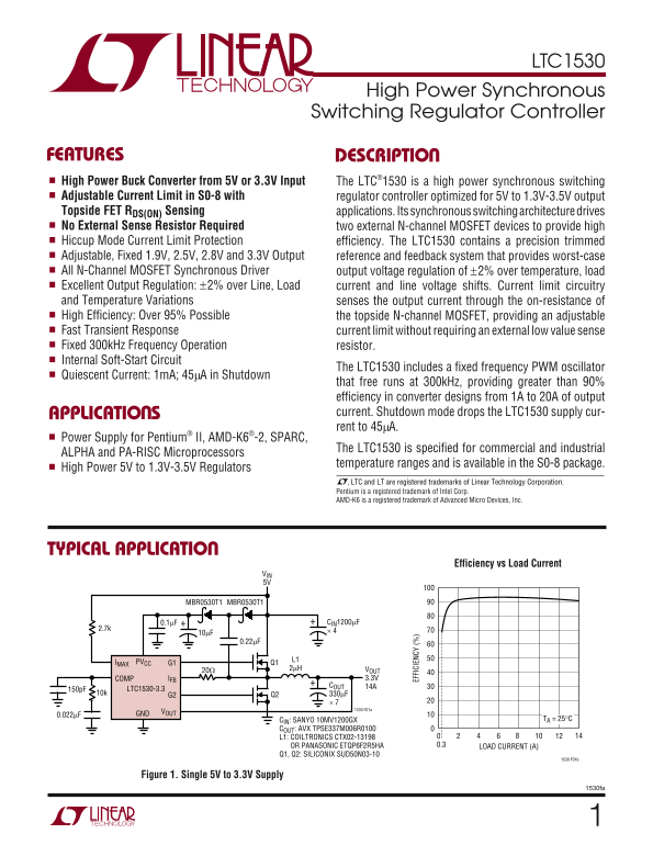
TYPICAL APPLICATIO

Efficiency vs Load Current

VIN 5V

MBR0530T1 MBR0530T1

0.1µF CIN1200µF

PVCC L1

IMAX G1 Q1

2µH VOUT

COMP IFB 3.3V

COUT 14A

150p F LTC1530-3.3

GND VOUT

CIN: SANYO 10MV1200GX TA = 25°C

COUT: AVX TPSE337M006R0100 L1: COILTRONICS CTX02-13198

OR PANASONIC ETQP6F2R5HA 0.3 LOAD CURRENT (A)

Q1, Q2: SILICONIX SUD50N03-10

Figure 1. Single 5V to 3.3V Supply

1530fa

Page Summary Contents For LINEAR TECHNOLOGY LTC1530 User's Manual

Page 1 LTC1530 High Power Synchronous Switching Regulator Controller FEATURES DESCRIPTIO High Power Buck Converter from 5V or 3.3V Input The LTC®1530 is a high power synchronous switching Adjustable Current ...
Page 2 LTC1530 ABSOLUTE AXI U RATI GS PACKAGE/ORDER I FOR ATIO (Note 1) ORDER PART Supply Voltage NUMBER PVCC 14V TOP VIEW Input Voltage LTC1530CS8 PVCC G1 IFB (Note 2) PVCC + 0.3V LTC1530CS8-1.9 GND G2 IMAX...
Page 3 LTC1530 ELECTRICAL CHARACTERISTICS The ● denotes specifications that apply over the full operating temperature range, otherwise specifications are at TA = 25°C. PVCC = 12V unless otherwise noted. (Not...
Page 4 UT (V UT (V EF FI CI EN CY LTC1530 TYPICAL PERFOR A CE CHARACTERISTICS Efficiency vs Load Current Load Regulation LTC1530 VSENSE vs Temperature TA = 25°C REFER TO FIGURE 2 2.496 (V 1.225 OU TP UT OL T...
Page 5 SH UT DO TH RE SH OL VO LT AG (m V) AX IN CU RR EN (µ A) ER RO AM PL IF IE OP EN -L OO DC AI (d B) LTC1530 TYPICAL PERFOR A CE CHARACTERISTICS Error Amplifier Open-Loop Gain Oscillator Frequency Maxim...
Page 6 LTC1530 PI FU CTIO S PVCC (Pin 1): Power Supply for G1, G2 and Logic. PVCC COMP to compensate the feedback loop for optimum must connect to a potential of at least VIN + VGS(ON)Q1. If transient respon...
Page 7 LTC1530 BLOCK DIAGRA DISDR LOGIC AND THERMAL SHUTDOWN INTERNAL OSCILLATOR POWER DOWN ICOMP FIXED VOUT R1 R2 gm = 2millimho ERR MIN MAX –+ VSENSE VREF VREF – 3% VREF + 3% R1 FB IFB R2 FOR FIXED CC VOLT...
Page 8 LTC1530 TEST CIRCUITS PVCC 12V tr tf IFB G1 G1 RISE/FALL 3300p F t SS t NOL t NOL LTC1530 COMPCOMP G2 G2 RISE/FALL 50% 50% VOUT GND 3300p F 1530 F04b Figure 4 APPLICATIO S I FOR ATIO OVERVIEW sawtooth...
Page 9 LTC1530 APPLICATIO S I FOR ATIO Typically, thermal shutdown is activated if the LTC1530’s By using the RDS(ON) of Q1 to measure output current, the junction temperature exceeds 150°C. G1 and G2 resume...
Page 10 LTC1530 APPLICATIO S I FOR ATIO Figure 5b plots the minimum required RIMAX resistor (kΩ) RIMAX ≥ 500Ω versus the maximum operating load current (ILMAX = ILMAX = ILOAD + IRIPPLE/2 ILOAD + IRIPPLE/2) as...
Page 11 LTC1530 APPLICATIO S I FOR ATIO In order for the current limit circuit to operate properly and Power MOSFETs to obtain a reasonably accurate current limit threshold, the Two N-channel power MOSFETs ar...
Page 12 LTC1530 APPLICATIO S I FOR ATIO either Q1 or Q2 with the power dissipation split up accord- Note that while the required RDS(ON) values suggest large ing to the duty cycle: MOSFETs, the power dissipat...
Page 13 LTC1530 APPLICATIO S I FOR ATIO Table 1. Recommended MOSFETs for LTC1530 Applications RDS(ON) TYPICAL INPUT AT 25°C RATED CURRENT CAPACITANCE θJC TJMAX MANUFACTURER PART NO. PACKAGE (Ω) (A) Ciss (p F)...
Page 14 LTC1530 APPLICATIO S I FOR ATIO circuits not employing the current limit function, the output load transient response, choose the output capaci- current in the inductor may rise above this maximum tor...
Page 15 LTC1530 APPLICATIO S I FOR ATIO LC 2π LTC1530 The ESR of the output capacitor and the output capacitor ERR value form a zero at the frequency: RC ESR 2π ESR OUT 1530 F08a The compensation network used...
Page 16 LTC1530 APPLICATIO S I FOR ATIO Table 3. Suggested Compensation Network for a 5V Input After achieving a satisfactory power path layout, pro- Application Using Multiple Paralleled 1500µF SANYO MV-GX c...
Page 17 LTC1530 APPLICATIO S I FOR ATIO BOLD LINES INDICATE HIGH CURRENT PATHS PVCC G1 Q1 CIN 0.1µF LTC1530 GND G2 RIFB LO IFB VOUT RIMAX COMP IMAX Q2 C1 0.1µF CC Figure 9. LTC1530 Layout Diagram VIN 5V 2.7k ...
Page 18 LTC1530 TYPICAL APPLICATIO S 5V to 1.9V-3.3V Synchronous Buck Converter PVCC Is Generated from Charge Pump VIN 5V MBR0530T1 MBR0530T1 0.1µF 10µF CIN** IMAX PVCC G1 Q1* LO VOUT COMP IFB 1.9V TO 3.3V CO...
Page 19 LTC1530 TYPICAL APPLICATIO S LTC1530 3.3V to 1.8V, 14A Application VIN 3.3V GND LTC1517-5 D2 MBRS120 D1 MBRS120 CIN 1500µF × 3 SUD50N03 PVCC L1 IMAX G1 2.5µH20Ω VOUT COMP IFB 1.8V C1 COUT RC 14A LTC15...
Page 20 LTC1530 TYPICAL APPLICATIO S LTC1530 High Efficiency Boost Converter 1µH VOUT MBRS140T3 330µF 330µF 330µF 1µF MBR0530T1 IRF7811 EF FI CI EN CY D1 Q3 Q4 FMMD914 IRF7811 IRF7811 10µF 1µF PVCC IMAX IFB 1...
Page 21 LTC1530 TYPICAL APPLICATIO S LTC1530 5V to –5V Synchronous Inverter VIN 5V OPTIONAL D1 R8 Z1 MBR0530T1 2.4k EF FI CI EN CY 1/2W 2.2µF ZENER LTC1693-2 MBR0530T1 C3 C4 PVCC IMAX G1 100Ω 330Ω Q2 VOUT 10µ...
Page 22 LTC1530 TYPICAL APPLICATIO S LTC1530 Synchronous SEPIC Converter RSENSE Q2 0.02ΩVIN L1A P-MOSFET VOUT VOUT 4V TO 8V CIN 10,11,12 Q1 COUT N-MOSFET R4 EF FI CI EN CY MBR0520 VIN IMAX IFBPVCC 4.7µF SHDN ...
Page 23 LTC1530 PACKAGE DESCRIPTION S8 Package 8-Lead Plastic Small Outline (Narrow 0.150) (LTC DWG # 05-08-1610) NOTE 3 .050 BSC MIN .150 – .157 NOTE 3 .030 ±.005 TYP RECOMMENDED SOLDER PAD LAYOUT (0.203 – 0...
Page 24 LTC1530 TYPICAL APPLICATION LTC1530 –5V to 2.5V, 5A Inverting Polarity Converter (OPTIONAL) Z1 MBRS130 MBRS130R8 1N4742A 4.7Ω 0.1µF RSENSE VOUT* L1 COUT 5A R6 R7 2.5µH 1500µF CIN 2k 22Ω 6.3V 1500µF × ...

Manual Details

Brand Linear
Pages 24
File Size 301.36 KB
Published June 06, 2026
52 views

Enter the captcha to get the download link:

captcha

Frequently Asked Questions

Is an external sense resistor required for current sensing?

No external sense resistor is required; it uses top-side FET sensing through the MOSFET on-resistance.

What protection features are built into the LTC1530?

It provides adjustable current limit and Hiccup Mode Current Limit Protection.

How does the device maintain high efficiency?

It achieves over 95% efficiency by using top-side N-channel MOSFET sensing technology.

What voltage options are available for the fixed output reference?

The chip offers precision trimmed, adjustable reference voltages of 1.9V, 2.5V, 2.8V, and 3.3V.