# A B C D E F G H I J K L M N O P Q R S T U V W X Y Z

LINEAR TECHNOLOGY LTC1484 User's Manual

Summary

This low-power RS485/RS422 transceiver is designed for reliable data communication in demanding residential and industrial environments. It features a fail-safe receiver that guarantees signal integrity, even when the input lines are open, shorted, or floating. The comprehensive manual details its advanced electrical specifications, includes robust ESD protection (–15kV), and outlines operational guidelines necessary for engineers building resilient bus systems supporting up to 32 transceivers.
📄 Preview PAGE OF 16

Page 1 Text Content

LTC1484 Low Power

RS485 Transceiver with Receiver Fail-Safe

FEATURES DESCRIPTIO

No Damage or Latchup to ±15k V ESD (Human The LTC®1484 is a low power RS485 compatible trans- Body Model), IEC-1000-4-2 Level 4 Contact (±8k V) ceiver. In receiver mode, it offers a fail-safe feature which and Level 3 (±8k V) Air Gap Specifications guarantees a high receiver output state when the inputs Guaranteed High Receiver Output State for Floating, are left open, shorted together or terminated with no

Shorted or Terminated Inputs with No Signal signal present. No external components are required to Present ensure the high receiver output state.

Drives Low Cost Residential Telephone Wires

Both driver and receiver feature three-state outputs with

Low Power: ICC = 700µA Max with Driver Disabled

separate receiver and driver control pins. The driver

ICC = 900µA Max for Driver Enable with No Load

outputs maintain high impedance over the entire com-

20µA Max Quiescent Current in Shutdown Mode

mon mode range when three-stated. Excessive power

Single 5V Supply

dissipation caused by bus contention or faults is pre-

–7V to 12V Common Mode Range Permits ±7V

vented by a thermal shutdown circuit that forces the

Ground Difference Between Devices on the Data Line

driver outputs into a high impedance state.

Power Up/Down Glitch-Free Driver Outputs

Up to 32 Transceivers on the Bus Enhanced ESD protection allows the LTC1484 to with- Pin Compatible with the LTC485 stand ±15k V (human body model), IEC-1000-4-2 level 4 Available in 8-Lead MSOP, PDIP and SO Packages (±8k V) contact and level 3 (±8k V) air discharge ESD without latchup or damage. The LTC1484 is fully specified over the commercial and

APPLICATIO

industrial temperature ranges and is available in 8-lead

Battery-Powered RS485/RS422 Applications MSOP, PDIP and SO packages.■ Low Power RS485/RS422 Transceiver

, LTC and LT are registered trademarks of Linear Technology Corporation.

Level Translator

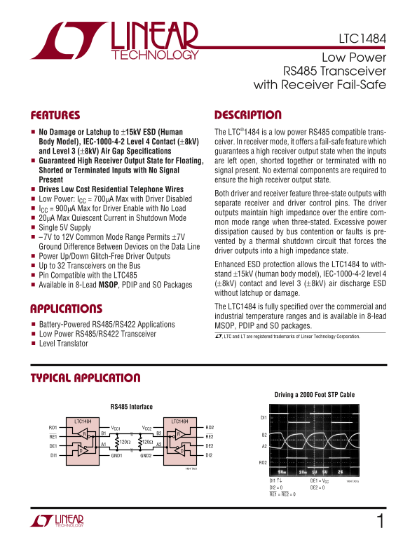
TYPICAL APPLICATIO

Driving a 2000 Foot STP Cable

RS485 Interface

LTC1484 LTC1484

RO1 VCC1 VCC2 RO2

RE1 RE2

DE1 DE2 A2

DI1 GND1 GND2 DI2

1484 TA01

Dl1 ↑↓ DE1 = VCC 1484 TA01a

Dl2 = 0 DE2 = 0 RE1 = RE2 = 0

Page Summary Contents For LINEAR TECHNOLOGY LTC1484 User's Manual

Page 1 LTC1484 Low Power RS485 Transceiver with Receiver Fail-Safe FEATURES DESCRIPTIO No Damage or Latchup to ±15k V ESD (Human The LTC®1484 is a low power RS485 compatible trans- Body Model), IEC-1000-4-2 ...
Page 2 LTC1484 ABSOLUTE MAXIMUM RATINGS (Note 1) Supply Voltage (VCC) 6.5V Junction Temperature 125°C Control Input Voltages –0.3V to (VCC + 0.3V) Operating Temperature Range Driver Input Voltage –0.3V to (V...
Page 3 LTC1484 ELECTRICAL CHARACTERISTICS The ● denotes the specifications which apply over the full operating temperature range, otherwise specifications are at TA = 25°C. VCC = 5V ±5% (Notes 2 and 3) unles...
Page 4 RE CE IV ER UT PU VO LT AG (V LTC1484 SWITCHING CHARACTERISTICS The ● denotes the specifications which apply over the full operating temperature range, otherwise specifications are at TA = 25°C. VCC =...
Page 5 RE CE IV ER UT PU LO OL TA GE (V RE CE IV ER UT PU HI GH OL TA GE (V RE CE IV ER IN PU OF FS ET OL TA GE (m V) LTC1484 TYPICAL PERFOR A CE CHARACTERISTICS Receiver Input Offset Voltage vs Receiver Hys...
Page 6 SU PP LY UR RE NT (µ A) RE CE IV ER RO PA GA TI ON EL AY (n s) RE CE IV ER HO RT -C IR CU IT UR RE NT (m A) LTC1484 TYPICAL PERFOR A CE CHARACTERISTICS Receiver Short-Circuit Current vs Receiver Propa...
Page 7 DR IV ER IF FE RE NT IA OU TP UT OL TA GE (V DR IV ER OM ON OD VO LT AG (V DR IV ER IF FE RE NT IA OU TP UT OL TA GE (V LTC1484 TYPICAL PERFOR A CE CHARACTERISTICS Driver Differential Output Voltage D...
Page 8 DR IV ER HO RT -C IR CU IT UR RE NT (m A) DR IV ER UT PU HI GH OL TA GE (V LTC1484 TYPICAL PERFOR A CE CHARACTERISTICS Driver Output High Voltage vs Driver Output Low Voltage vs Driver Propagation Del...
Page 9 LTC1484 PIN FUNCTIONS A (Pin 6): Driver Output/Receiver Input. The input resis- B (Pin 7): Driver Output/Receiver Input. The input resis- tance is typically 22k when the driver is disabled (DE = 0). t...
Page 10 LTC1484 SWITCHI G TI E WAVEFOR S 3V DI 1.5V f = 1MHz, tr ≤ 10ns, tf ≤ 10ns 1.5V t PLH t PHL VO = V(A) – V(B) tr tf 1/2 VO t SKEW t SKEW NOTE: DE = 1 Figure 6. Driver Propagation Delays DE 1.5V f = 1MH...
Page 11 LTC1484 SWITCHI G TI E WAVEFOR S 3V DE 1.5V f = 1MHz, tr ≤ 10ns, tf ≤ 10ns t DZR OUTPUT NORMALLY LOW RO 1.5V OUTPUT NORMALLY HIGH NOTE: DI = 0, RE = 0, A AND B ARE THREE-STATED WHEN DE = 0 Figure 10. ...
Page 12 LTC1484 APPLICATIONS INFORMATION Shutdown Mode temperatures, the rise in die temperature due to the short-circuit current may trip the thermal shutdown The receiver output (RO) and the driver outputs ...
Page 13 LTC1484 APPLICATIONS INFORMATION RO4 DE4 RO2DE2 1k 1k DE1 RO3DE3RO1 Figure 11. Transmit “0” CDMA Application receiver output and expects to see perfect agreement Figure 12a shows a 100k Hz DE1 wavefor...
Page 14 LTC1484 APPLICATIONS INFORMATION longer delay for the falling edge is due to the larger voltage pull-down resistors. However, if the resistors are left out, range the line must swing (typically >2V...
Page 15 LTC1484 PACKAGE DESCRIPTION Dimensions in inches (millimeters), unless otherwise noted. N8 Package 8-Lead PDIP (Narrow 0.300) (LTC DWG # 05-08-1510) 0.400* (10.160) MAX 0.065 (1.651) 0.009 – 0.015 TYP...
Page 16 LTC1484 TYPICAL APPLICATIO Fail-Safe “0” Application (Idle State = Logic “0”) LTC1484 RO RO I1 VCC RE “A” DE “B” DI I2 GND 1484 TA02 RELATED PARTS PART NUMBER DESCRIPTION COMMENTS LTC485 5V Low Power ...

Manual Details

Brand Linear
Pages 16
File Size 224.93 KB
Published June 17, 2026
2 views

Enter the captcha to get the download link:

captcha

Frequently Asked Questions

What fail-safe feature does the LTC1484 guarantee in receiver mode?

It guarantees a high receiver output state regardless of whether the inputs are left open, shorted together, or terminated with no signal present.

Can the LTC1484 drive multiple transceivers on the bus?

Yes, it supports up to 32 Transceivers on the Bus.

Does the device require external components for its fail-safe feature?

No, no external components are required to ensure the high receiver output state.