# A B C D E F G H I J K L M N O P Q R S T U V W X Y Z

LINEAR TECHNOLOGY LTC1286 LTC1298 User's Manual

Summary

These micropower 12-bit A/D converters are designed for high-precision data acquisition in varied environments. Ideal for battery monitoring, remote sensing, or medical applications, they utilize low power consumption (down to 1nA standby) and feature options like differential inputs and multi-channel multiplexing. The accompanying manual provides detailed technical specifications, operating parameters, and application guidelines necessary for engineers building reliable, low-maintenance data logging systems.
📄 Preview PAGE OF 24

Page 1 Text Content

LTC1286/LTC1298 Micropower Sampling 12-Bit A/D Converters In S0-8 Packages

FEATURES DESCRIPTION 12-Bit Resolution The LTC1286/LTC1298 are micropower, 12-bit, succes- 8-Pin SOIC Plastic Package sive approximation sampling A/D converters. They typi- Low Cost cally draw only 250µA of supply current when converting Low Supply Current: 250µA Typ. and automatically power down to a typical supply current Auto Shutdown to 1n A Typ. of 1n A whenever they are not performing conversions. Guaranteed ±3/4LSB Max DNL They are packaged in 8-pin SO packages and operate on Single Supply 5V to 9V Operation 5V to 9V supplies. These 12-bit, switched-capacitor, suc- On-Chip Sample-and-Hold cessive approximation ADCs include sample-and-holds. 60µs Conversion Time The LTC1286 has a single differential analog input. The Sampling Rates: LTC1298 offers a software selectable 2-channel MUX.

12.5 ksps (LTC1286)

On-chip serial ports allow efficient data transfer to a wide

11.1 ksps (LTC1298)

range of microprocessors and microcontrollers over three

I/O Compatible with SPI, Microwire, etc.

wires. This, coupled with micropower consumption, makes

Differential Inputs (LTC1286)

remote location possible and facilitates transmitting data

SU PP LY UR RE NT (µ A)

2-Channel MUX (LTC1298)

through isolation barriers.

3V Versions Available: LTC1285/LTC1288

These circuits can be used in ratiometric applications or

APPLICATIONS with an external reference. The high impedance analog

inputs and the ability to operate with reduced spans (to

Battery-Operated Systems

1.5V full scale) allow direct connection to sensors and

Remote Data Acquisition

transducers in many applications, eliminating the need for

Battery Monitoring

gain stages.

Handheld Terminal Interface Temperature Measurement Isolated Data Acquisition

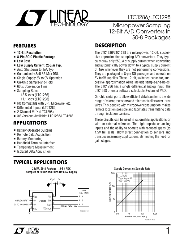
TYPICAL APPLICATIONS N 25µW, S0-8 Package, 12-Bit ADC Supply Current vs Sample Rate Samples at 200Hz and Runs Off a 5V Supply

TA = 25°C VCC = VREF = 5V

f CLK = 200k Hz

MPU (e.g., 8051)

VREF VCC P1.4

ANALOG INPUT +IN LTC1286 CLK P1.3 0V TO 5V RANGE –IN DOUT P1.2

SERIAL DATA LINK

GND CS/SHDN

LTC1286/98 • TA01

0.1k 1k 10k 100k SAMPLE FREQUENCY (Hz)

LTC1286/98 • TA02

Page Summary Contents For LINEAR TECHNOLOGY LTC1286 LTC1298 User's Manual

Page 1 LTC1286/LTC1298 Micropower Sampling 12-Bit A/D Converters In S0-8 Packages FEATURES DESCRIPTION 12-Bit Resolution The LTC1286/LTC1298 are micropower, 12-bit, succes- 8-Pin SOIC Plastic Package sive ap...
Page 2 LTC1286/LTC1298 ABSOLUTE MAXIMUM RATINGS (Notes 1 and 2) Supply Voltage (VCC) to GND................................... 12V Power Dissipation 500m W Voltage Operating Temperature Range Analog and Refe...
Page 3 LTC1286/LTC1298 CONVERTER AND MULTIPLEXER CHARACTERISTICS (Note 5) LTC1286 LTC1298 PARAMETER CONDITIONS MIN TYP MAX MIN TYP MAX UNITS Resolution (No Missing Codes) Bits Integral Linearity Error (Note ...
Page 4 SU PP LY UR RE NT (µ A) LTC1286/LTC1298 AC CHARACTERISTICS (Note 5) SYMBOL PARAMETER CONDITIONS MIN TYP MAX UNITS t SMPL Analog Input Sample Time See Operating Sequence 1.5 CLK Cycles f SMPL(MAX) Maxi...
Page 5 CH AN GE IN FF SE (L SB RE FE RE NC CU RR EN (µ A) AD NO IS IN BS LTC1286/LTC1298 TYPICAL PERFORMANCE CHARACTERISTICS Reference Current vs Change in Offset vs Sample Rate (LTC1286) Reference Current v...
Page 6 AG NI TU DE (d B) CL OC FR EQ UE NC (k Hz SP UR IO US RE DY NA IC AN GE d B LTC1286/LTC1298 TYPICAL PERFORMANCE CHARACTERISTICS Spurious Free Dynamic Range Attenuation vs vs Frequency S/(N+D) vs Input...
Page 7 CL OC FR EQ UE NC (k Hz LTC1286/LTC1298 TYPICAL PERFORMANCE CHARACTERISTICS Minimum Clock Frequency Digital Input Logic Threshold Input Channel Leakage Current for 0.1 LSB Error vs Temperature vs Supp...
Page 8 LTC1286/LTC1298 BLOCK DIAGRAM CS/SHDN (DIN) CLK VCC (VCC/VREF) BIAS AND SERIAL PORT DOUT SHUTDOWN CIRCUIT IN+ (CH0) CSAMPLE IN– (CH1) MICROPOWER COMPARATOR CAPACITIVE DAC VREF PIN NAMES IN PARENTHESES...
Page 9 LTC1286/LTC1298 TEST CIRCUITS Voltage Waveforms for tdis Voltage Waveforms for ten LTC1286 CS VIH WAVEFORM 1 (SEE NOTE 1) 1CLK DOUT WAVEFORM 2 (SEE NOTE 2) B11 NOTE 1: WAVEFORM 1 IS FOR AN OUTPUT WITH...
Page 10 LTC1286/LTC1298 APPLICATION INFORMATION SERIAL INTERFACE A/D conversion result is output on the DOUT line. Bringing CS high resets the LTC1286 for the next data exchange. The 2-channel LTC1298 communi...
Page 11 LTC1286/LTC1298 APPLICATION INFORMATION DIN 1 DIN 2 DOUT 1 DOUT 2 SHIFT MUX ADDRESS IN 1 NULL BIT SHIFT A/D CONVERSION RESULT OUT LTC1096/98 • AI01 MSB-First Data (MSBF = 0) t CYC tsu CS POWER DOWN ST...
Page 12 LTC1286/LTC1298 REF REF –1LSB APPLICATION INFORMATION REF –2LSB Input Data Word MSBF bit is a logical zero, LSB first data will follow the normal MSB first data on the DOUT line. (see Operating The LT...
Page 13 LTC1286/LTC1298 SU PP LY UR RE NT (µ A) APPLICATION INFORMATION MSBF BIT LATCHED CS BY LTC1298 DATA (DIN/DOUT) START SGL/DIFF ODD/SIGN MSBF B11 B10 MPU CONTROLS DATA LINE AND SENDS LTC1298 CONTROLS DA...
Page 14 LTC1286/LTC1298 SU PP LY UR RE NT (µ A) APPLICATION INFORMATION Clock Frequency TA = 25°C VCC = VREF = 5V The maximum recommended clock frequency is 200k Hz for the LTC1286/LTC1298 running off a 5V su...
Page 15 LTC1286/LTC1298 APPLICATION INFORMATION BOARD LAYOUT CONSIDERATIONS SAMPLE-AND-HOLD Both the LTC1286 and the LTC1298 provide a built-in Grounding and Bypassing sample-and-hold (S&H) function to ac...
Page 16 LTC1286/LTC1298 APPLICATION INFORMATION Differential Inputs sample time can be increased by using a slower CLK frequency. With differential inputs, the ADC no longer converts just a single voltage but...
Page 17 LTC1286/LTC1298 APPLICATION INFORMATION will slow the settling of the inputs. It is important that the converter, the reference input should be driven by a overall RC time constants be short enough to...
Page 18 LTC1286/LTC1298 APPLICATION INFORMATION 0.2V reference. If this offset is unacceptable, it can be tortion and noise at the rated throughput. By applying a low corrected digitally by the receiving syst...
Page 19 LTC1286/LTC1298 EF FE CT IV NU BE OF IT (E NO Bs APPLICATION INFORMATION If two pure sine waves of frequencies fa and fb are applied to the ADC input, nonlinearities in the ADC transfer func- tion can...
Page 20 LTC1286/LTC1298 TYPICAL APPLICATIONS N MICROPROCESSOR INTERFACES The LTC1286/LTC1298 can interface directly without ex- Table 1. Microprocessor with Hardware Serial Interfaces Compatible with the LTC1...
Page 21 LTC1286/LTC1298 TYPICAL APPLICATIONS N Timing Diagram for Interface to the MC68HC11 DIN MSBF DON'T CAREODD/ DIFFSTART SIGN TRANSMIT MSBF XODD/ XX0 XX XX DIFF SIGN BYTE 1 BYTE 3 (DUMMY)BYTE 2 RECEIVED ...
Page 22 LTC1286/LTC1298 TYPICAL APPLICATIONS N Interfacing to the Parallel Port of the INTEL 8051 LABEL MNEMONIC OPERAND COMMENTS Family MOV A, #FFH DIN word for LTC1298 SETB P1.4 Make sure CS is high The Int...
Page 23 LTC1286/LTC1298 TYPICAL APPLICATIONS N A “Quick Look” Circuit for the LTC1286 Users can get a quick look at the function and timing of the Micropower Battery Voltage Monitor LT1286 by using the follow...
Page 24 LTC1286/LTC1298 Dimensions in inches (millimeters) unless otherwise noted.PACKAGE DESCRIPTION N8 Package 8-Lead Plastic DIP (7.620 – 8.128) (1.143 – 1.651) (3.302 ± 0.127) MAX 0.009 – 0.015 TYP 0.250 ...

Manual Details

Brand Linear
Pages 24
File Size 286.88 KB
Published June 02, 2026
71 views

Enter the captcha to get the download link:

captcha

Frequently Asked Questions

What is the maximum sampling rate available?

The LTC1298 offers a software selectable range up to 11.1 ksamples per second (ksps).

Is battery power compatible with this unit?

Yes, it can operate down to a full scale of 1.5V, making connection to sensors and transducers possible without extra battery monitoring stages.

How does the LTC1286 handle analog inputs?

It has a single differential analog input that allows for remote data acquisition and uses its built-in sample-and-hold circuit.

What is the operational temperature range for all components?

The Analog and Reference components operate from 0°C to 70°C, while the Digital Inputs are rated for -40°C to 85°C.