# A B C D E F G H I J K L M N O P Q R S T U V W X Y Z

LINEAR TECHNOLOGY LTC1155 User's Manual

Summary

LTC1155 is a dual high-side micropower MOSFET driver enabling N-channel FETs for high-side switching. Features internal charge pump, 8uA standby, 85uA operating current, 4.5-18V supply, overcurrent protection, and short-circuit shutdown. In 8-pin PDIP/SO, it targets laptop, cellular phone, and battery-powered system designers needing efficient power switching.
📄 Preview PAGE OF 16

Page 1 Text Content

LTC1155

Dual High Side

Micropower MOSFET Driver SFEATURE ESCRIPTIO

Fully Enhances N-Channel Power MOSFETs The LTC®1155 dual high side gate driver allows using low 8µA Standby Current cost N-channel FETs for high side switching applications. 85µA ON Current An internal charge pump boosts the gate above the posi- Short-Circuit Protection tive rail, fully enhancing an N-channel MOSFET with no Wide Power Supply Range: 4.5V to 18V external components. Micropower operation, with 8µA

Controlled Switching ON and OFF Times standby current and 85µA operating current, allows use in

No External Charge Pump Components virtually all systems with maximum efficiency. Replaces P-Channel High Side MOSFETs

Included on-chip is overcurrent sensing to provide auto-

Compatible with Standard Logic Families

matic shutdown in case of short circuits. A time delay can

Available in 8-Pin SO Package

be added in series with the current sense to prevent false triggering on high in-rush loads such as capacitors and PPLICATI SA incandescent lamps. Laptop Power Bus Switching The LTC1155 operates off of a 4.5V to 18V supply input SCSI Termination Power Switching and safely drives the gates of virtually all FETs. The Cellular Phone Power Management LTC1155 is well suited for low voltage (battery-powered) P-Channel Switch Replacement applications, particularly where micropower “sleep” op-

Relay and Solenoid Drivers VO LT AG DR OP (V eration is required. Low Frequency Half H-Bridge

The LTC1155 is available in both 8-pin PDIP and 8-pin SO

Motor Speed and Torque Control

packages. , LTC and LT are registered trademarks of Linear Technology Corporation.

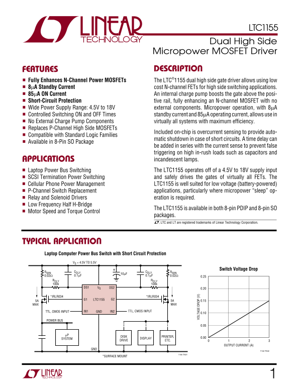
PPLICATITYPICAL Laptop Computer Power Bus Switch with Short Circuit Protection VS = 4.5V TO 5.5V

Switch Voltage Drop

RSEN CDLY CDLY RSEN

RDLY RDLY 100k 100k

DS2VSDS1 0.20

*IRLR034 *IRLR034

G1 LTC1155 G2

5A 5A 0.15 MAX MAX

GNDIN1 IN2 TTL, CMOS INPUTTTL, CMOS INPUT

POWER BUS

DISK PRINTER,

DISPLAY 0.00

SYSTEM

DRIVE ETC.

OUTPUT CURRENT (A)

1155 TA02

1155 TA01

*SURFACE MOUNT

Page Summary Contents For LINEAR TECHNOLOGY LTC1155 User's Manual

Page 1 LTC1155 Dual High Side Micropower MOSFET Driver SFEATURE ESCRIPTIO Fully Enhances N-Channel Power MOSFETs The LTC®1155 dual high side gate driver allows using low 8µA Standby Current cost N-channel FE...
Page 2 LTC1155 XI ARBSOLUTE TI (Note 1) Supply Voltage 22V Operating Temperature Range Input Voltage (VS +0.3V) to (GND – 0.3V) LTC1155C................................................ 0°C to 70°C Gate Volta...
Page 3 IN PU TH RE SH OL VO LT AG (V SU PP LY UR RE NT LTC1155 ELECTRICAL CHARA TERISTICS The ● denotes the specifications which apply over the full operating temperature range, otherwise specifications are ...
Page 4 SU PP LY UR RE NT (µ A) TU RN -O TI (µ s) LTC1155 PERFOR ATYPICAL CE CHARA TERISTICS Turn ON Time Turn OFF Time Short-Circuit Turn OFF Delay Time CGATE = 1000p F CGATE = 100p F CGATE = 1000p F TIME FO...
Page 5 LTC1155 PIN FUNCTIONS The supply pin of the LTC1155 should not be forced below This pin is also a high impedance CMOS gate with ESD ground as this may result in permanent damage to the protection and,...
Page 6 LTC1155 OPERATIO Gate Charge Pump lead. If the drop across this resistor exceeds the internal 100m V threshold, the input latch is reset and the gate is Gate drive for the power MOSFET is produced by ...
Page 7 LTC1155 PPLICATI SA FOR ATIO For this example, we assume a worst-case scenario; i.e., Graphical Approach to Selecting RDLY and CDLY that the power supply to the power MOSFET is “hard” and Figure 2 is ...
Page 8 LTC1155 PPLICATI SA FOR ATIO VS = 5.0V If the MOSFET is turned ON and the power supply (battery) removed, the inductor current is delivered by the supply CDLY RSEN 0.22µF 0.025Ω capacitor. The supply ...
Page 9 LTC1155 PPLICATI SA FOR ATIO VS = 4.5V TO 18V 18.6V and pulls the drain sense pin 0.6V below the supply pin voltage. CDLY RSEN The supply voltage is limited to 18.6V and the gate drive is immediately ...
Page 10 LTC1155 PPLICATITYPICAL SA X-NOR Fault Detection High Side Driver with VDS Sense Short-Circuit Shutdown 4.5V TO 6V 4.5V TO 6V VS VS 5V DS1 DS1 IN1 IN1 LTC1155 LTC1155 10k G1 IRLZ24 G1 IRLD024 GND GND ...
Page 11 LTC1155 PPLICATITYPICAL SA Automotive High Side Driver with Reverse-Battery 5V/3A Extremely Low Voltage Drop Regulator with 10µA Standby and High Voltage Transient Protection Current and Short-Circuit...
Page 12 LTC1155 PPLICATITYPICAL SA Logic Controlled Boost Mode Switching Regulator with Short-Circuit Protection and 8µA Standby Current 4.75V TO 5.25V FROM µP, ETC. IN1 LTC1155 G1 MTM25N05L GND 5V SWITCHED F...
Page 13 LTC1155 PPLICATITYPICAL SA High Efficiency 60Hz Full-Wave Synchronous Rectifier 9V/3A DC 4 × IRFZ44* DS1VSDS2 G1IN1 6.3V AC110V AC LT1006 LTC1155 IN2 G2 GND 1155 TA14 MOSFETs ARE SYNCHRONOUSLY ENHANCE...
Page 14 LTC1155 PPLICATITYPICAL SA Full H-Bridge Driver with Shoot-Through Current Lockout and Stall Current Shutdown (f O < 100Hz) 4.5V TO 6V DIRECTION 74HC02 DS2VSDS1 G1IN1 IRLZ44 IRLZ44 LTC1155 IN2 G2 V...
Page 15 LTC1155 PACKAGE DESCRIPTIO Dimensions in inches (milimeters) unless otherwise noted. J8 Package 8-Lead CERDIP (Narrow 0.300, Hermetic) (LTC DWG # 05-08-1110) 0.300 BSC CORNER LEADS OPTION (0.762 BSC) ...
Page 16 LTC1155 PPLICATITYPICAL SA Isolated High Voltage High Side Switch with Circuit Breaker 6V TO 12V 1/6 74C14 1k CONTROL DS2VSDS1 10µF G1IN1 6A MAX 100p F 1N4148 LTC1155 1N5817 IN2 MUR420 1155 TA18 Isola...

Manual Details

Brand Linear
Pages 16
File Size 268.64 KB
Published June 15, 2026
2 views

Enter the captcha to get the download link:

captcha

Frequently Asked Questions

What is the supply voltage range of the LTC1155?

The LTC1155 operates from a 4.5V to 18V supply input.

Does the LTC1155 require external charge pump components?

No, it has an internal charge pump and needs no external charge pump components.

What protection does the LTC1155 offer for short circuits?

It has on-chip overcurrent sensing to provide automatic shutdown in case of short circuits.

What packages is the LTC1155 available in?

It is available in 8-pin PDIP and 8-pin SO packages.