# A B C D E F G H I J K L M N O P Q R S T U V W X Y Z

LINEAR TECHNOLOGY LTC1096 LTC1096L User Guide Manual

Summary

These ultra-low power 8-bit Analog-to-Digital Converters (ADCs) are engineered for demanding remote and battery-powered systems, making them ideal for data acquisition and advanced telemetry. The line includes both 3V and 5V versions designed to draw minimal current, even in standby mode, facilitating isolated signal monitoring like battery health gauging. This manual provides comprehensive technical specifications, application guides, and operational parameters for integrating the LTC1096/LTC1098 series with microprocessors and microcontrollers needing highly reliable ADC conversion performance.
📄 Preview PAGE OF 28

Page 1 Text Content

LTC1096/LTC1096L LTC1098/LTC1098L Micropower Sampling

8-Bit Serial I/O A/D Converters

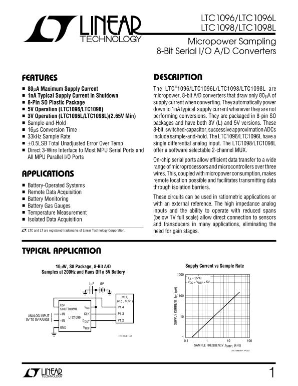
ESCRIPTIOSFEATURE 80µA Maximum Supply Current The LTC®1096/LTC1096L/LTC1098/LTC1098L are 1n A Typical Supply Current in Shutdown micropower, 8-bit A/D converters that draw only 80µA of 8-Pin SO Plastic Package supply current when converting. They automatically power 5V Operation (LTC1096/LTC1098) down to 1n A typical supply current whenever they are not 3V Operation (LTC1096L/LTC1098L)(2.65V Min) performing conversions. They are packaged in 8-pin SO Sample-and-Hold packages and have both 3V (L) and 5V versions. These 16µs Conversion Time 8-bit, switched-capacitor, successive approximation ADCs 33k Hz Sample Rate include sample-and-hold. The LTC1096/LTC1096L have a ±0.5LSB Total Unadjusted Error Over Temp single differential analog input. The LTC1098/LTC1098L Direct 3-Wire Interface to Most MPU Serial Ports and offer a software selectable 2-channel MUX.

All MPU Parallel I/O Ports

On-chip serial ports allow efficient data transfer to a wide range of microprocessors and microcontrollers over three PPLICATI SA wires. This, coupled with micropower consumption, makes

SU PP LY UR RE NT , I CC (µ A)

remote location possible and facilitates transmitting data

Battery-Operated Systems

through isolation barriers.

Remote Data Acquisition

These circuits can be used in ratiometric applications or

Battery Monitoring

with an external reference. The high impedance analog

Battery Gas Gauges

inputs and the ability to operate with reduced spans

Temperature Measurement

(below 1V full scale) allow direct connection to sensors

Isolated Data Acquisition

and transducers in many applications, eliminating the

, LTC and LT are registered trademarks of Linear Technology Corporation.

need for gain stages.

PPLICATITYPICAL

10µW, S8 Package, 8-Bit A/D Supply Current vs Sample Rate

Samples at 200Hz and Runs Off a 5V Battery

TA = 25°C VCC = VREF = 5V

MPU (e.g., 8051)

VCC P1.4

SHUTDOWN

+IN CLK P1.3

ANALOG INPUT

LTC1096

0V TO 5V RANGE P1.2

–IN DOUT

GND VREF

LTC1096/8 • TA01

0.1 SAMPLE FREQUENCY, f SMPL (k Hz)

LTC1096/98 • TPC03

Page Summary Contents For LINEAR TECHNOLOGY LTC1096 LTC1096L User Guide Manual

Page 1 LTC1096/LTC1096L LTC1098/LTC1098L Micropower Sampling 8-Bit Serial I/O A/D Converters ESCRIPTIOSFEATURE 80µA Maximum Supply Current The LTC®1096/LTC1096L/LTC1098/LTC1098L are 1n A Typical Supply Curre...
Page 2 LTC1096/LTC1096L LTC1098/LTC1098L XI ARBSOLUTE TI (Notes 1 and 2) Supply Voltage (VCC) to GND................................... 12V Operating Temperature Voltage LTC1096AC/LTC1096C/LTC1096LC/ Analog ...
Page 3 LTC1096/LTC1096L LTC1098/LTC1098L RECO E DED OPERATI G CO DITIO S LTC1096/LTC1098 SYMBOL PARAMETER CONDITIONS MIN TYP MAX UNITS t WLCLK CLK Low Time VCC = 5V 0.8 µs t WHCS CS High Time Between Data Tr...
Page 4 LTC1096/LTC1096L LTC1098/LTC1098L CO VERTER A D ULTIPLEXER CHARACTERISTICS LTC1096/LTC1098 VCC = 5V, VREF = 5V, f CLK = 500k Hz, unless otherwise noted. LTC1096/LTC1098LTC1096A/LTC1098A PARAMETER COND...
Page 5 LTC1096/LTC1096L LTC1098/LTC1098L DIGITAL AND DC ELECTRICAL CHARACTERISTICS LTC1096/LTC1098 VCC = 5V, VREF = 5V, unless otherwise noted. SYMBOL PARAMETER CONDITIONS MIN TYP MAX UNITS VIH High Level In...
Page 6 LTC1096/LTC1096L LTC1098/LTC1098L DIGITAL AND DC ELECTRICAL CHARACTERISTICS LTC1096L/LTC1098L VCC = 2.65V, VREF = 2.5V, f CLK = 250k Hz, unless otherwise noted. SYMBOL PARAMETER CONDITIONS MIN TYP MAX...
Page 7 LTC1096/LTC1096L LTC1098/LTC1098L AC CHARACTERISTICS LTC1096/LTC1098 VCC = 3V, VREF = 2.5V, f CLK = 250k Hz, unless otherwise noted. SYMBOL PARAMETER CONDITIONS MIN TYP MAX UNITS t SMPL Analog Input S...
Page 8 LTC1096/LTC1096L AG NI TU DE OF FS ET HA NG (L SB /2 RE F) SU PP LY UR RE NT , I (µ A) CH AN GE IN IN EA RT (L SB CC LTC1098/LTC1098L PERFOR ATYPICAL CE CHARA TERISTICS Supply Current vs Clock Rate Su...
Page 9 LTC1096/LTC1096L IN IM UM LO CK RE QU EN CY (k Hz AK E- UP IM (µ s) AX IM UM LO CK RE QU EN CY (M Hz LTC1098/LTC1098L PERFOR ATYPICAL CE CHARA TERISTICS Maximum Clock Frequency vs Maximum Clock Freque...
Page 10 LTC1096/LTC1096L LTC1098/LTC1098L PI FU CTIO S LTC1096/LTC1096L LTC1098/LTC1098L CS/SHDN (Pin 1): Chip Select Input. A logic low on this CS/SHDN (Pin 1): Chip Select Input. A logic low on this input e...
Page 11 LTC1096/LTC1096L LTC1098/LTC1098L TEST CIRCUITS On and Off Channel Leakage Current Load Circuit for td DO, tr and tf 5V ON CHANNEL DOUT TEST POINT POLARITY LTC1096/98 • TC1 Voltage Waveforms for DOUT ...
Page 12 LTC1096/LTC1096L LTC1098/LTC1098L TEST CIRCUITS Voltage Waveforms for ten LTC1096/LTC1096L t WAKEUP LTC1098/LTC1098L ten LTC1096/98 • TC07 DIN START LTC1096/98 • TC08 PPLICATI SA FOR ATIO OVERVIEW a s...
Page 13 LTC1096/LTC1096L LTC1098/LTC1098L PPLICATI SA FOR ATIO t WAKEUP Power Down and Wake-Up Time The LTC1096(L)/LTC1098(L) draw power when the CS pin is low and shut themselves down when that pin is high. ...
Page 14 LTC1096/LTC1096L LTC1098/LTC1098L PPLICATI SA FOR ATIO MSB-FIRST DATA (MSBF = 1) t CYC POWER DOWN t WAKEUP tsu CS ODD/ START SIGN DIN DON'T CARE SGL/ MSBF HI-Z NULL Hi-Z DOUT BIT B0*B1B2B3B4B5B6B7 (MS...
Page 15 LTC1096/LTC1096L LTC1098/LTC1098L REF PPLICATI SA FOR ATIO REF –1LSB the A/D conversion result is output on the DOUT line. MSB-First/LSB-First (MSBF) REF –2LSB Bringing CS high resets the LTC1096(L) f...
Page 16 LTC1096/LTC1096L LTC1098/LTC1098L SU PP LY UR RE NT , I CC (µ A) PPLICATI SA FOR ATIO MSBF BIT LATCHED CS BY LTC1098(L) DATA (DIN/DOUT) START SGL/DIFF ODD/SIGN MSBF B7 B6 MPU CONTROLS DATA LINE AND SE...
Page 17 LTC1096/LTC1096L LTC1098/LTC1098L PPLICATI SA FOR ATIO the converter will draw current. This current may be larger Wake-Up Time than the typical supply current. It is worthwhile to bring the A 10µs wa...
Page 18 LTC1096/LTC1096L LTC1098/LTC1098L PPLICATI SA FOR ATIO (Figure 6) and connect the center point to the MPU input. The VCC pin should be bypassed to the ground plane with It should be noted that to get ...
Page 19 LTC1096/LTC1096L LTC1098/LTC1098L PPLICATI SA FOR ATIO in and continues until the falling CLK edge after the MSBF t WAKEUP or t SMPL for the LTC1096(L) or the LTC1098(L) + and C1 will improve bit is r...
Page 20 LTC1096/LTC1096L LTC1098/LTC1098L PPLICATI SA FOR ATIO cycle. Large external source resistors and capacitances tive current spike will be generated on the reference pin by will slow the settling of th...
Page 21 LTC1096/LTC1096L LTC1098/LTC1098L PPLICATI SA FOR ATIO reference voltage for a typical value of VOS. For example, settle within the bit time at which the clock is running. a VOS of 2m V which is 0.1LS...
Page 22 LTC1096/LTC1096L LTC1098/LTC1098L PPLICATI SA FOR ATIO Effective Number of Bits f SAMPLE = 31.25k Hz The effective number of bits (ENOBs) is a measurement of the resolution of an A/D and is directly r...
Page 23 LTC1096/LTC1096L LTC1098/LTC1098L PPLICATITYPICAL SA Data Exchange Between LTC1098(L) and MC68HC05C4 START BIT BYTE 1 BYTE 2 (DUMMY) MPU TRANSMIT SGL/ ODD/ WORD DIFF SIGN X = DON'T CARE START SGL/ ODD...
Page 24 LTC1096/LTC1096L LTC1098/LTC1098L PPLICATITYPICAL SA Interfacing to the Parallel Port of the LABEL MNEMONIC OPERAND COMMENTS Intel 8051 Family MOV A, #FFH DIN word for LTC1098(L) SETB P1.4 Make sure C...
Page 25 LTC1096/LTC1096L LTC1098/LTC1098L PPLICATITYPICAL SA A “Quick Look” Circuit for the LTC1096 Users can get a quick look at the function and timing of the LT1096 by using the following simple circuit (F...
Page 26 LTC1096/LTC1096L LTC1098/LTC1098L PPLICATITYPICAL SA Remote or Isolated Systems conversions and the optoisolators draw power only when data is being transferred. The system consumes only Figure 16 sho...
Page 27 LTC1096/LTC1096L LTC1098/LTC1098L PACKAGE DESCRIPTIO Dimensions in inches (millimeters), unless otherwise noted. N8 Package 8-Lead PDIP (Narrow 0.300) (LTC DWG # 05-08-1510) 0.400* (10.160) MAX 0.255 ...
Page 28 LTC1096/LTC1096L LTC1098/LTC1098L PPLICATITYPICAL A/D Conversion for 3V Systems The LTC1096/LTC1098 are ideal for 3V systems. Figure 17 LT1004 provides the full-scale reference for the ADC. The shows ...

Manual Details

Brand Linear
Pages 28
File Size 368.93 KB
Published May 30, 2026
82 views

Enter the captcha to get the download link:

captcha

Frequently Asked Questions

What is the typical supply current when idle or in shutdown?

The device automatically powers down to a typical supply current of 1nA when not performing conversions.

Which models are available for use with 3V systems?

The LTC1096L and LTC1098L versions are available for operation at 3V (2.65V Min).

How does the LTC1098 model differ from the LTC1096?

The LTC1098 offers a software selectable 2-channel MUX, while the LTC1096 does not advertise this feature.

What kind of data interface do these converters have?

They include a direct 3-Wire Interface for most MPUs (Serial) and all MPU Parallel I/O ports.