# A B C D E F G H I J K L M N O P Q R S T U V W X Y Z

LINEAR TECHNOLOGY - LTC1052 LTC7652 Data Sheet Manual

Summary

These zero-drift operational amplifiers (LTC1052/LTC7652) deliver unparalleled precision for demanding analog applications, featuring guaranteed low offset drift and ultra-low noise performance. Designed with chopper-stabilization technology, they ensure exceptional long-term stability crucial for sensing high-accuracy signals. This manual provides detailed technical specifications, operating guidelines, electrical characteristics, and application support necessary for integrating these amplifiers into medical instrumentation or specialized signal processing circuits.
📄 Preview PAGE OF 24

Page 1 Text Content

LTC1052/LTC7652 Zero-Drift Operational Amplifier

FEATURES DESCRIPTIO Guaranteed Max Offset: 5µV The LTC®1052 and LTC7652 are low noise zero-drift op Guaranteed Max Offset Drift: 0.05µV/°C amps manufactured using Linear Technology’s enhanced Typ Offset Drift: 0.01µV/°C LTCMOSTM silicon gate process. Chopper-stabilization Excellent Long Term Stability: 100n V/√Month constantly corrects offset voltage errors. Both initial offset Guaranteed Max Input Bias Current: 30p A and changes in the offset due to time, temperature and Over Operating Temperature Range: common mode voltage are corrected. This, coupled with Guaranteed Min Gain: 120d B picoampere input currents, gives these amplifiers Guaranteed Min CMRR: 120d B unmatched performance. Guaranteed Min PSRR: 120d B

Low frequency (1/f) noise is also improved by the

Single Supply Operation: 4.75V to 16V

chopping technique. Instead of increasing continuously

(Input Voltage Range Extends to Ground)

at a 3d B/octave rate, the internal chopping causes noise to

External Capacitors can be Returned to V– with No

decrease at low frequencies.

Noise Degradation

VO LT AG NO IS DE NS IT (n V/ √H z)

The chopper circuitry is entirely internal and completely transparent to the user. Only two external capacitors

APPLICATIO S

are required to alternately sample-and-hold the offset ■ Thermocouple Amplifiers correction voltage and the amplified input signal. Control ■ Strain Gauge Amplifiers circuitry is brought out on the 14-pin and 16-pin versions to allow the sampling of the LTC1052 to be synchronized

Low Level Signal Processing

with an external frequency source.

Medical Instrumentation

, LTC and LT are registered trademarks of Linear Technology Corporation. LTCMOS is a trademark of Linear Technology Corporation.

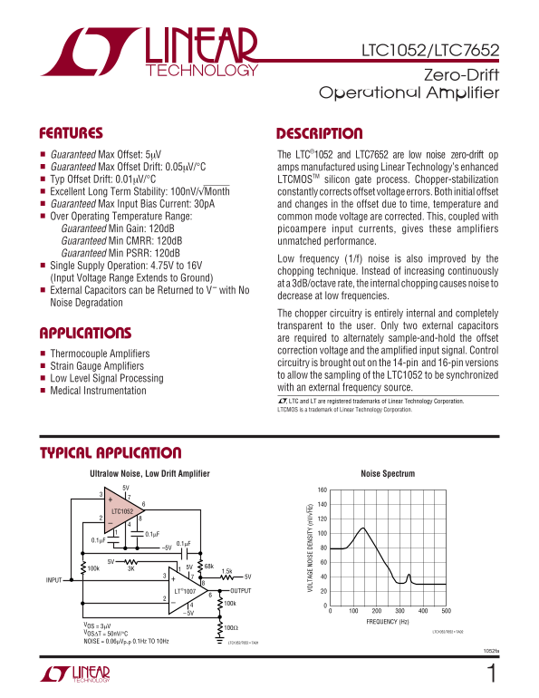
TYPICAL APPLICATIO Ultralow Noise, Low Drift Amplifier Noise Spectrum

LTC1052

INPUT

LT®1007 OUTPUT

FREQUENCY (Hz)

VOS = 3µV

VOS∆T = 50n V/°C LTC1052/7652 • TA02

NOISE = 0.06µVP-P 0.1Hz TO 10Hz LTC1052/7652 • TA01

1052fa

Page Summary Contents For LINEAR TECHNOLOGY - LTC1052 LTC7652 Data Sheet Manual

Page 1 LTC1052/LTC7652 Zero-Drift Operational Amplifier FEATURES DESCRIPTIO Guaranteed Max Offset: 5µV The LTC®1052 and LTC7652 are low noise zero-drift op Guaranteed Max Offset Drift: 0.05µV/°C amps manufac...
Page 2 LTC1052/LTC7652 ABSOLUTE AXI U RATI GS (Notes 1 and 2) Total Supply Voltage (V+ to V–) 18V Operating Temperature Range Input Voltage (V+ + 0.3V) to (V– – 0.3V) LTC1052C/LTC7652C .........................
Page 3 LTC1052/LTC7652 ELECTRICAL CHARACTERISTICS The ● denotes the specifications which apply over the full operating temperature range, otherwise specifications are at TA = 25°C. VS = ±5V, test circuit TC1...
Page 4 OU TP UT PE CT RU (d B) PHASE SHIFT (DEGREES)180 (µ V) LTC1052/LTC7652 OU TP UT OL TA GE (2 0m V/ DI V) (3 Hz AN DW ID TH TYPICAL PERFOR A CE CHARACTERISTICS Offset Voltage vs Sampling 1OHz P-P Noise ...
Page 5 SA PL IN FR EQ UE NC Y, (H z) SU PP LY UR RE NT , I A) IN PU RE FE RR ED OI SE LTC1052/LTC7652 (5 µV /D IV TYPICAL PERFOR A CE CHARACTERISTICS Broadband Noise, CEXT = 0.1µF Broadband Noise, CEXT = 1.0...
Page 6 LTC1052/LTC7652 TYPICAL PERFOR A CE CHARACTERISTICS Response Time vs Overdrive VREF + OVERDRIVE INPUT{ VREF – 1m V OUTPUT 5µV 20ms/DIV TEST CIRCUITS Electrical Characteristics Test Circuit (TC1) DC to...
Page 7 LTC1052/LTC7652 THEORY OF OPERATIO power supply are also nulled. For nulling to take place, the For frequencies above this pole, I2 is: offset voltage, common mode voltage and power supply I2 = VIN gm...
Page 8 LTC1052/LTC7652 THEORY OF OPERATIO gm1 gm2 gm4 gm5 VOUT IN l1 RL1 RL2 CEXT B RL4 CEXT A gm6 LTC1052/7652 • TO02 Figure 1b. LTC1052 Block Diagram Sampling Cycle APPLICATIO S I FOR ATIO EXTERNAL CAPACIT...
Page 9 LTC1052/LTC7652 APPLICATIO S I FOR ATIO connections, to the inverting input. Guarding both sides Figure 2 is an example of the introduction of an of the printed circuit board is required. Bulk leakage...
Page 10 LTC1052/LTC7652 APPLICATIO S I FOR ATIO When all of these errors are considered, it may seem Figure 4 shows the response of this circuit under impossible to take advantage of the extremely low drift t...
Page 11 LTC1052/LTC7652 APPLICATIO S I FOR ATIO #1 COVERED #1 UNCOVERED #2 UNCOVERED 20 SEC Figure 5. DC to 1Hz (Test Circuit TC3) PACKAGE-INDUCED OFFSET VOLTAGE CLOCK Since the LTC1052 is constantly fixing i...
Page 12 LTC1052/LTC7652 APPLICATIO S I FOR ATIO OUTPUT CLAMP within approximately 1V of either supply rail. This switch is in parallel with the amplifier’s feedback resistor. As the If the LTC1052 is driven i...
Page 13 LTC1052/LTC7652 TYPICAL APPLICATIO S Offset Stabilized Comparator 5V COMPARATOR COMPARATOR LT1011 INPUTS OUTPUT (± 5V) GROUND OR 1µF INPUT COMMON- MODE VOLTAGE LTC1043 5V LTC1052 5V STATUS OUTPUT 5V O...
Page 14 LTC1052/LTC7652 TYPICAL APPLICATIO S No VOS Adjust* CMOS DAC Buffer—Single Supply Air Flow Detector 15V CF* 10k 5V RFB 1k 15V l OUT1 12–BIT CMOS DAC LTC1052 VOUT 1% l OUT2 FOR HIGHER SPEED, REFER TO “...
Page 15 LTC1052/LTC7652 TYPICAL APPLICATIO S ±100m A Output Drive Increasing Output Current LTC1052 LTC1010 VOUT INPUT OUTPUT LTC1052 VOS 5µV VOS/∆T 50µV/°C LOAD OUTPUT SWING 100Ω FULL POWER BANDWIDTH 1k Hz L...
Page 16 LTC1052/LTC7652 TYPICAL APPLICATIO S Increasing Output Current and Voltage (VSUPPLY = ±15V) DC Stabilized FET Probe INPUT CAPACITANCE BOOTSTRAP 5V FAST SOURCE Q1 FOLLOWER INPUT 3k NC INPUT LT1010 OUTP...
Page 17 LTC1052/LTC7652 TYPICAL APPLICATIO S Direct Thermocouple-to-Frequency Converter COLD JUNCTION TEMPERATURE TRACKING STABILIZING AMPTYPE K 1.8k* 470Ω THERMOCOUPLE 41.4µV/°C 5V 33k BA EDC10k 100k 1N914 L...
Page 18 LTC1052/LTC7652 TYPICAL APPLICATIO S 16-Bit A/D Converter CLOCK 0.01µF BOUT EIN 95k* 1/3 74C903 OV TO 5V LTC1052 1/2 74C74 FULL-SCALE TRIM AOUT INTEGRATOR 2N4338 LTC1052 LT1009 75k* 20k LINEARITY TRIM...
Page 19 LTC1052/LTC7652 TYPICAL APPLICATIO S Precision Isolation Amplifier 1k* OUTPUT SIDEINPUT SIDE 20k ZERO TRIM 15V 15V LTC1052 100k 14–PIN L2 STANCOR PCT-39 LTC1052 OUT1000p F 2N54342N5434 1k GAIN TRIM IN...
Page 20 LTC1052/LTC7652 PACKAGE DESCRIPTIO H Package 8-Lead TO-5 Metal Can (.200 Inch PCD) (Reference LTC DWG # 05-08-1320) .335 – .370 (8.509 – 9.398) DIA .305 – .335 (7.747 – 8.509) MAX (1.270) .165 – .185 ...
Page 21 LTC1052/LTC7652 PACKAGE DESCRIPTIO J Package 14-Lead CERDIP (Narrow .300 Inch, Hermetic) (Reference LTC DWG # 05-08-1110) .785 (19.939) MAX.005 (0.127) MIN RAD TYP .300 BSC (7.62 BSC) BSC.014 – .026 N...
Page 22 LTC1052/LTC7652 PACKAGE DESCRIPTIO J8 Package 8-Lead CERDIP (Narrow .300 Inch, Hermetic) (Reference LTC DWG # 05-08-1110) CORNER LEADS OPTION .405 (4 PLCS) (10.287) (0.127) MIN .023 – .045 (0.584 – 1....
Page 23 LTC1052/LTC7652 PACKAGE DESCRIPTIO N Package 14-Lead PDIP (Narrow .300 Inch) (Reference LTC DWG # 05-08-1510) .770* (19.558) MAX MIN .065 (0.203 – 0.381) TYP –0.3818.255( MIN MIN (2.54) BSC NOTE: INCH...
Page 24 LTC1052/LTC7652 PACKAGE DESCRIPTIO SW Package 16-Lead Plastic Small Outline (Wide .300 Inch) (Reference LTC DWG # 05-08-1620) .050 BSC.030 ±.005 .045 ±.005 .398 – .413 TYP (10.109 – 10.490) NOTE 4 NOT...

Manual Details

Brand Linear
Pages 24
File Size 848.24 KB
Published May 25, 2026
161 views

Enter the captcha to get the download link:

captcha

Frequently Asked Questions

What does the device guarantee regarding long-term offset stability?

It provides a guaranteed max offset drift of 0.05µV/°C and excellent stability corrected by chopper-stabilization.

What is the required external components for basic operation?

Only two external capacitors are required to alternately sample-and-hold the offset correction voltage and the amplified input signal.

What are the standard absolute operating temperature specifications?

The LTC1052C/LTC7652C modules operate in a range of –40°C to 85°C. The 'M' variants can handle -55°C to 125°C.

What is the specified guaranteed minimum common-mode rejection ratio (CMRR)?

The LTC1052/LTC7652 provides a minimum guaranteed CMRR of 120dB.