# A B C D E F G H I J K L M N O P Q R S T U V W X Y Z

LINEAR TECHNOLOGY - LT6220 LT6221 LT6222 Data Sheet User Manual

Summary

These multi-channel operational amplifiers are designed for high-speed, low-power signal processing requiring exceptional performance in low voltage applications. The manual provides comprehensive details on single, dual, and quad configurations, covering critical features like 60MHz bandwidth, rail-to-rail I/O, wide supply range (2.2V–12.6V), and ultra-low quiescent current. They are essential for circuit designers developing high-frequency analog systems in compact or battery-powered devices where efficiency and precision are paramount.
📄 Preview PAGE OF 20

Page 1 Text Content

LT6220/LT6221/LT6222 Single/Dual/Quad 60MHz,

20V/µs, Low Power, Rail-to-Rail Input and Output Precision Op Amps

FEATURES DESCRIPTIO Gain Bandwidth Product: 60MHz The LT®6220/LT6221/LT6222 are single/dual/quad, low

Input Common Mode Range Includes Both Rails power, high speed rail-to-rail input and output operational Output Swings Rail-to-Rail amplifiers with excellent DC performance. The LT6220/

Low Quiescent Current: 1m A Max LT6221/LT6222 feature reduced supply current, lower Input Offset Voltage: 350µV Max input offset voltage, lower input bias current and higher Input Bias Current: 150n A Max DC gain than other devices with comparable bandwidth. Wide Supply Range: 2.2V to 12.6V

Typically, the LT6220/LT6221/LT6222 have an input off-

Large Output Current: 50m A Typ

set voltage of less than 100µV, an input bias current of less

Low Voltage Noise: 10n V√Hz Typ

than 15n A and an open-loop gain of 100V/m V. The parts

Slew Rate: 20V/µs Typ

have an input range that includes both supply rails and an

Common Mode Rejection: 102d B Typ

output that swings within 10m V of either supply rail to maxi-

Power Supply Rejection: 105d B Typ

mize the signal dynamic range in low supply applications.

Open-Loop Gain: 100V/m V Typ

Operating Temperature Range: – 40°C to 85°C The LT6220/LT6221/LT6222 maintain performance for Single in the 8-Pin SO and 5-Pin Low Profile PE RC EN OF NI TS supplies from 2.2V to 12.6V and are specified at 3V, 5V (1mm) Thin SOTTM Packages and ±5V supplies. The inputs can be driven beyond the Dual in the 8-Pin SO and (3mm x 3mm) DFN supplies without damage or phase reversal of the output.

Packages

The LT6220 is housed in the 8-pin SO package with the

Quad in the 16-Pin SSOP Package

standard op amp pinout as well as the 5-pin SOT-23 package. The LT6221 is available in 8-pin SO and DFN

APPLICATIO S

(3mm × 3mm low profile dual fine pitch leadless) pack- ages with the standard op amp pinout. The LT6222 fea-

Low Voltage, High Frequency Signal Processing

tures the standard quad op amp configuration and is

Driving A/D Converters

available in the 16-Pin SSOP package. The LT6220/ LT6221/

Rail-to-Rail Buffer Amplifiers

LT6222 can be used as plug-in replacements for many op

Active Filters

amps to improve input/output range and performance.

Video Amplifiers

, LTC and LT are registered trademarks of Linear Technology Corporation.

Fast Current Sensing Amplifiers

Thin SOT is a trademark of Linear Technology Corporation.

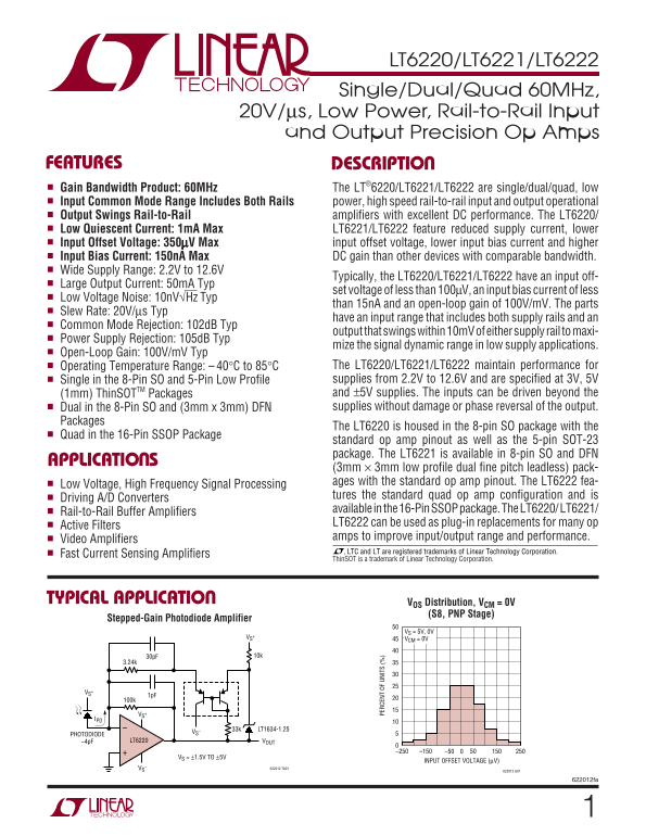
TYPICAL APPLICATIO VOS Distribution, VCM = 0V

(S8, PNP Stage)

Stepped-Gain Photodiode Amplifier

VS = 5V, 0V

VS+ VCM = 0V

33k LT1634-1.25

PHOTODIODE

~4p F LT6220 VOUT

VS = ±1.5V TO ±5V

INPUT OFFSET VOLTAGE (µV)

VS– 622012 TA01

622012fa

Page Summary Contents For LINEAR TECHNOLOGY - LT6220 LT6221 LT6222 Data Sheet User Manual

Page 1 LT6220/LT6221/LT6222 Single/Dual/Quad 60MHz, 20V/µs, Low Power, Rail-to-Rail Input and Output Precision Op Amps FEATURES DESCRIPTIO Gain Bandwidth Product: 60MHz The LT®6220/LT6221/LT6222 are single/d...
Page 2 LT6220/LT6221/LT6222 ABSOLUTE AXI RATI GS (Note 1) – to VS Total Supply Voltage (VS 12.6V Maximum Junction Temperature 150°C Input Voltage (Note 2) ±VS (DD Package) 125°C Input Current (Note 2) ±10m A...
Page 3 LT6220/LT6221/LT6222 ELECTRICAL CHARACTERISTICS TA = 25°C, VS = 5V, 0V; VS = 3V, 0V; VCM = VOUT = half supply, unless otherwise noted SYMBOL PARAMETER CONDITIONS MIN TYP MAX UNITS VOS Input Offset Vol...
Page 4 LT6220/LT6221/LT6222 ELECTRICAL CHARACTERISTICS The ● denotes the specifications which apply over the 0°C ≤ TA ≤ 70°C temperature range. VS = 5V, 0V; VS = 3V, 0V; VCM = VOUT = half supply, unless othe...
Page 5 LT6220/LT6221/LT6222 ELECTRICAL CHARACTERISTICS The ● denotes the specifications which apply over the –40°C ≤ TA ≤ 85°C temperature range. VS = 5V, 0V; VS = 3V, 0V; VCM = VOUT = half supply unless oth...
Page 6 LT6220/LT6221/LT6222 ELECTRICAL CHARACTERISTICS TA = 25°C, VS = ±5V, VCM = 0V, VOUT = 0V, unless otherwise noted. SYMBOL PARAMETER CONDITIONS MIN TYP MAX UNITS VOS Input Offset Voltage VCM = –5V µV VC...
Page 7 LT6220/LT6221/LT6222 ELECTRICAL CHARACTERISTICS The ● denotes the specifications which apply over the 0°C ≤ TA ≤ 70°C temperature range. VS = ±5V, VCM = 0V, VOUT = 0V, unless otherwise noted. SYMBOL P...
Page 8 LT6220/LT6221/LT6222 ELECTRICAL CHARACTERISTICS The ● denotes the specifications which apply over the –40°C ≤ TA ≤ 85°C temperature range. VS = ±5V, VCM = 0V, VOUT = 0V, unless otherwise noted. (Note ...
Page 9 IN PU BI AS UR RE NT (n A) PE RC EN OF NI TS PE RC EN OF NI TS LT6220/LT6221/LT6222 TYPICAL PERFOR A CE CHARACTERISTICS VOS Distribution, VCM = 0V VOS Distribution, VCM = 0V VOS Distribution, VCM = 5V...
Page 10 CH AN GE IN FF SE VO LT AG (m V) CH AN GE IN FF SE VO LT AG (µ V) OU TP UT AT UR AT IO VO LT AG (V LT6220/LT6221/LT6222 TYPICAL PERFOR A CE CHARACTERISTICS Output Saturation Voltage Output Short-Circu...
Page 11 IN (d PHASE M B) ARGIN (DEG) GA IN AN DW ID TH (M Hz NO IS CU RR EN (p A/ √H z) LT6220/LT6221/LT6222 TYPICAL PERFOR A CE CHARACTERISTICS Gain Bandwidth and Phase Input Current Noise vs Frequency 0.1Hz...
Page 12 OU TP UT OL TA GE IN (V P- P) OV ER SH OO CO ON OD RE JE CT IO RA TI (d B) LT6220/LT6221/LT6222 TYPICAL PERFOR A CE CHARACTERISTICS Common Mode Rejection Ratio Power Supply Rejection Ratio Series Outp...
Page 13 LT6220/LT6221/LT6222 TYPICAL PERFOR A CE CHARACTERISTICS ±5V Large-Signal Response ±5V Small-Signal Response Output Overdriven Recovery VIN 1V/DIV 2V/DIV 50m V/DIV VOUT 2V/DIV 0V VS = ±5V 200ns/DIV 62...
Page 14 LT6220/LT6221/LT6222 APPLICATIO S I FOR ATIO A pair of complementary common emitter stages Q14/Q15 Input Offset Voltage that enable the output to swing from rail-to-rail construct The offset voltage w...
Page 15 LT6220/LT6221/LT6222 APPLICATIO S I FOR ATIO severely overdriven, an external resistor should be used to capacitive load, a resistor of 10Ω to 50Ω should be limit the overdriven current. connected bet...
Page 16 LT6220/LT6221/LT6222 PACKAGE DESCRIPTIO As the signal level increases though, the output of the op amp goes more negative. At 12.5µA of photodiode cur- rent, the 100kΩ gain dictates that the LT6220 ou...
Page 17 LT6220/LT6221/LT6222 PACKAGE DESCRIPTIO and the output of the lower path is: rise to the effective differential gain of 2. Calculations show that using 1% resistors gives worst-case input common +OUT ...
Page 18 LT6220/LT6221/LT6222 PACKAGE DESCRIPTIO S5 Package 5-Lead Plastic TSOT-23 (Reference LTC DWG # 05-08-1635) 2.90 BSC MAX REF (NOTE 4) 1.22 REF 3.85 MAX 1.4 MIN2.62 REF (NOTE 4)2.80 BSC PIN ONE RECOMMEN...
Page 19 LT6220/LT6221/LT6222 PACKAGE DESCRIPTIO S8 Package 8-Lead Plastic Small Outline (Narrow .150 Inch) (Reference LTC DWG # 05-08-1610) NOTE 3 .050 BSC MIN .150 – .157 NOTE 3 .030 ±.005 TYP RECOMMENDED SO...
Page 20 LT6220/LT6221/LT6222 TYPICAL APPLICATIO VICM + VDIFF/2 R4 VS 1/4 LT6222 1/4 LT6222 VICM – VDIFF/2 –IN +OUT 1/4 LT6222 1/4 LT6222 R7 VS 2k VS = ±1.3V TO ±6V BW ≅ 11MHz Figure 6. Buffered Gain of 2 Diff...

Manual Details

Brand Linear
Pages 20
File Size 281.15 KB
Published June 16, 2026
6 views

Enter the captcha to get the download link:

captcha

Frequently Asked Questions

What is the general operating voltage range for these op amps?

They typically support a wide supply range from 2.2V to 12.6V.

Do these amplifiers handle low signal levels accurately at the output?

Yes, they feature rail-to-rail input and output capabilities, maintaining performance down to 10mV of either supply rail.

What are the available configurations for this device series?

The parts come in single (LT6220), dual (LT6221), or quad (LT6222) op amp configurations.

Are these components suitable for various temperature environments?

The standard operating temperature range is specified from –40°C to 85°C.