LINEAR TECHNOLOGY LT6220 LT6221 LT6222 Single Dual Quad 60MHz, 20V µs, Low Power, Rail-to-Rail Input and Output Precision Op Amps User Manual Specifications
Summary
Discover the LT622x series of high-performance, low-quiescent current operational amplifiers. Ideal for mission-critical signal processing in constrained power environments, these op-amps deliver exceptional rail-to-rail performance up to 60MHz across a wide supply range (2.2V–12.6V). Engineers utilizing the LT62xx series will find detailed technical specifications and application guidance within this manual. This resource is essential for designers building high-frequency data acquisition systems, active filters, or precision video amplifiers requiring reliable performance in low-voltage applications.
Page 1 Text Content
LT6220/LT6221/LT6222 Single/Dual/Quad 60MHz,
20V/µs, Low Power, Rail-to-Rail Input and Output Precision Op Amps
FEATURES DESCRIPTIO Gain Bandwidth Product: 60MHz The LT®6220/LT6221/LT6222 are single/dual/quad, low
Input Common Mode Range Includes Both Rails power, high speed rail-to-rail input and output operational Output Swings Rail-to-Rail amplifiers with excellent DC performance. The LT6220/
Low Quiescent Current: 1m A Max LT6221/LT6222 feature reduced supply current, lower Input Offset Voltage: 350µV Max input offset voltage, lower input bias current and higher Input Bias Current: 150n A Max DC gain than other devices with comparable bandwidth. Wide Supply Range: 2.2V to 12.6V
Typically, the LT6220/LT6221/LT6222 have an input off-
Large Output Current: 50m A Typ
set voltage of less than 100µV, an input bias current of less
Low Voltage Noise: 10n V√Hz Typ
than 15n A and an open-loop gain of 100V/m V. The parts
Slew Rate: 20V/µs Typ
have an input range that includes both supply rails and an
Common Mode Rejection: 102d B Typ
output that swings within 10m V of either supply rail to maxi-
Power Supply Rejection: 105d B Typ
mize the signal dynamic range in low supply applications.
Open-Loop Gain: 100V/m V Typ
Operating Temperature Range: – 40°C to 85°C The LT6220/LT6221/LT6222 maintain performance for Single in the 8-Pin SO and 5-Pin Low Profile PE RC EN OF NI TS supplies from 2.2V to 12.6V and are specified at 3V, 5V (1mm) Thin SOTTM Packages and ±5V supplies. The inputs can be driven beyond the Dual in the 8-Pin SO and (3mm x 3mm) DFN supplies without damage or phase reversal of the output.
Packages
The LT6220 is housed in the 8-pin SO package with the
Quad in the 16-Pin SSOP Package
standard op amp pinout as well as the 5-pin SOT-23 package. The LT6221 is available in 8-pin SO and DFN
APPLICATIO S
(3mm × 3mm low profile dual fine pitch leadless) pack- ages with the standard op amp pinout. The LT6222 fea-
Low Voltage, High Frequency Signal Processing
tures the standard quad op amp configuration and is
Driving A/D Converters
available in the 16-Pin SSOP package. The LT6220/ LT6221/
Rail-to-Rail Buffer Amplifiers
LT6222 can be used as plug-in replacements for many op
Active Filters
amps to improve input/output range and performance.
Video Amplifiers
, LTC and LT are registered trademarks of Linear Technology Corporation.
Fast Current Sensing Amplifiers
Thin SOT is a trademark of Linear Technology Corporation.
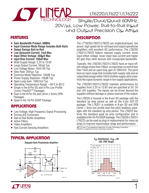
TYPICAL APPLICATIO VOS Distribution, VCM = 0V
(S8, PNP Stage)
Stepped-Gain Photodiode Amplifier
VS = 5V, 0V
VS+ VCM = 0V
33k LT1634-1.25
PHOTODIODE
~4p F LT6220 VOUT
VS = ±1.5V TO ±5V
INPUT OFFSET VOLTAGE (µV)
VS– 622012 TA01
622012fa
Page Summary Contents For LINEAR TECHNOLOGY LT6220 LT6221 LT6222 Single Dual Quad 60MHz, 20V µs, Low Power, Rail-to-Rail Input and Output Precision Op Amps User Manual Specifications
Manual Details
| Brand | Linear |
|---|---|
| Pages | 20 |
| File Size | 277.82 KB |
| Published | June 05, 2026 |
Enter the captcha to get the download link:

Frequently Asked Questions
What is the operating temperature range for these op amps?
The operating temperature range is –40°C to 85°C.
Can this device handle single and dual supply voltages?
Yes, it operates with both single and differential supplies from 2.2V to 12.6V.
What are the maximum performance specifications (Gain Bandwidth Product, Slew Rate)?
The Gain Bandwidth Product is 60MHz (Typ) and the Slew Rate is up to 20V/µs (Typ).
Are these op amps suitable for low supply applications?
Yes, they feature Common Mode Rejection of 102dB Typ and Power Supply Rejection of 105dB Typ.
Which packages are available for the LT6220/LT6221/LT6222 series?
These parts are available in various packages, including SO, DFN, ThinSOT-23, and SSOP.