LINEAR TECHNOLOGY LT1632 LT1633 sn1632 16323fs 45MHz, 45V μs, Dual Quad Rail-to-Rail Input and Output Precision Op Amps Owner's Manual - Specifications User Guide - Quick Setup
Summary
These precision op amplifiers are ideal for high-performance analog circuits requiring extreme reliability and wide operational range. Featuring a 45MHz gain-bandwidth product, rail-to-rail I/O, and low noise, they maintain performance across single or dual supplies (2.7V to 36V). The manual provides comprehensive specifications spanning application examples—including active filters, buffers, and A/D converter drivers—enabling designers to implement advanced signal processing in demanding, battery-powered systems.
Page 1 Text Content
LT1632/LT1633
45MHz, 45V/µs, Dual/Quad Rail-to-Rail Input and Output Precision Op Amps
FEATURES DESCRIPTION Gain-Bandwidth Product: 45MHz The LT®1632/LT1633 are dual/quad, rail-to-rail input and Slew Rate: 45V/µs output op amps with a 45MHz gain-bandwidth product and Low Supply Current per Amplifier: 4.3m A a 45V/µs slew rate. Input Common Mode Range Includes Both Rails
The LT1632/LT1633 have excellent DC precision over the
Output Swings Rail-to-Rail
full range of operation. Input offset voltage is typically less
Input Offset Voltage, Rail-to-Rail: 1350µV Max
than 400µV and the minimum open-loop gain of 0.8
Input Offset Current: 440n A Max
million into a 10k load virtually eliminates all gain error.
Input Bias Current: 2.2µA Max
Common mode rejection is typically 83d B over the full rail-
Open-Loop Gain: 800V/m V Min
to-rail input range when on a single 5V supply for excellent
Low Input Noise Voltage: 12n V/√Hz Typ
noninverting performance.
Low Distortion: – 92d Bc at 100k Hz
Wide Supply Range: 2.7V to ±15V The LT1632/LT1633 maintain their performance for sup- Large Output Drive Current: 35m A Min plies from 2.7V to 36V and are specified at 3V, 5V and ±15V
Dual in 8-Pin PDIP and SO Packages VO LT AG GA IN (d B) supplies. The inputs can be driven beyond the supplies
without damage or phase reversal of the output. The output delivers load currents in excess of 35m A.
APPLICATIONS
The LT1632 is available in 8-pin PDIP and SO packages
Active Filters
with the standard dual op amp pinout. The LT1633 features
Rail-to-Rail Buffer Amplifiers
the standard quad op amp configuration and is available in
Driving A/D Converters
a 14-pin plastic SO package. These devices can be used as
Low Voltage Signal Processing
plug-in replacements for many standard op amps to
Battery-Powered Systems
improve input/output range and performance. , LTC and LT are registered trademarks of Linear Technology Corporation.
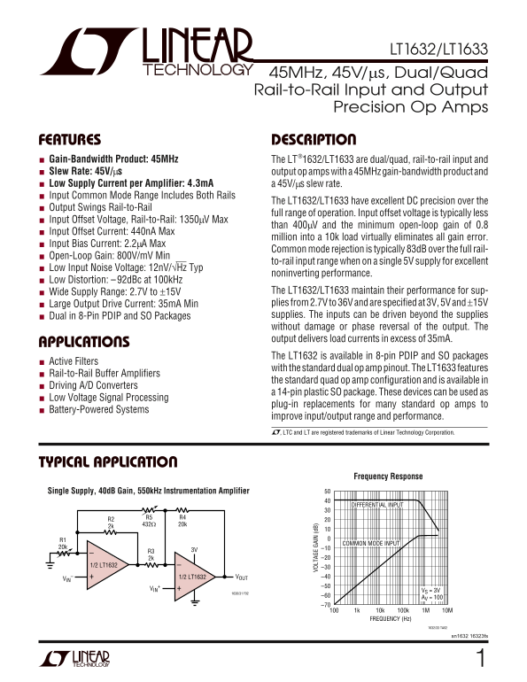
TYPICAL APPLICATION
Frequency Response
Single Supply, 40d B Gain, 550k Hz Instrumentation Amplifier
DIFFERENTIAL INPUT
COMMON MODE INPUT
1/2 LT1632
–30 1/2 LT1632 VOUT –40
VS = 3V
–60 AV = 100 –70
1k 10k 100k 1M 10M FREQUENCY (Hz)
1632/33 TA02
sn1632 16323fs
Page Summary Contents For LINEAR TECHNOLOGY LT1632 LT1633 sn1632 16323fs 45MHz, 45V μs, Dual Quad Rail-to-Rail Input and Output Precision Op Amps Owner's Manual - Specifications User Guide - Quick Setup
Manual Details
| Brand | Linear |
|---|---|
| Pages | 16 |
| File Size | 286.97 KB |
| Published | June 03, 2026 |
Enter the captcha to get the download link:

Frequently Asked Questions
What are the key specifications of the LT1632/LT1633?
They feature a 45MHz gain-bandwidth product, 45V/ms slew rate, and a low supply current of 4.3mA per amplifier.
How does the device perform with varying voltage supplies?
It maintains performance over a wide supply range of 2.7V to 36V, and the inputs can be driven beyond the supply rails.
Is this device suitable for various applications like signal processing or battery systems?
Yes, it can be used in active filters, rail-to-rail buffer amplifiers, and low voltage signal processing plug-in replacements for battery-powered systems.