LINEAR TECHNOLOGY LT1800 sn1800 1800fs 80MHz, 25V µs Low Power Rail-to-Rail Input and Output Precision Op Amp User Manual
Summary
The LT1800 is a high-speed, low-power operational amplifier designed for demanding signal processing applications requiring rail-to-rail operation and precision. This manual provides comprehensive details on the device’s electrical characteristics, performance specifications, and diverse application guidelines. Ideal for engineers designing energy-efficient systems—such as active filters, data acquisition buffer amplifiers, or video line drivers—who need reliable high-frequency amplification across varying single power supply levels (e.g., 2.3V to 12.6V).
Page 1 Text Content
LT1800
80MHz, 25V/µs Low Power Rail-to-Rail Input and Output Precision Op Amp
FEATURES DESCRIPTIO Gain Bandwidth Product: 80MHz The LT®1800 is a low power, high speed rail-to-rail input Input Common Mode Range Includes Both Rails and output operational amplifier with excellent DC perfor- Output Swings Rail-to-Rail mance. The LT1800 features reduced supply current, lower Low Quiescent Current: 2m A Max input offset voltage, lower input bias current and higher Input Offset Voltage: 350µV Max DC gain than other devices with comparable bandwidth. Input Bias Current: 250n A Max
The LT1800 has an input range that includes both supply
Low Voltage Noise: 8.5n V/√Hz
rails and an output that swings within 20m V of either sup-
Slew Rate: 25V/µs
ply rail to maximize the signal dynamic range in low supply
Common Mode Rejection: 105d B
applications.
Power Supply Rejection: 97d B
Open-Loop Gain: 85V/m V The LT1800 maintains its performance for supplies from Available in the 8-Pin SO and 5-Pin Low Profile 2.3V to 12.6V and is specified at 3V, 5V and ±5V supplies. (1mm) Thin SOTTM Packages The inputs can be driven beyond the supplies without Operating Temperature Range: –40°C to 85°C damage or phase reversal of the output. The LT1800 is available in the 8-pin SO package with the standard op amp pinout and in the 5-pin SOT-23 package.
APPLICATIO S
For dual and quad versions of the LT1800, see the LT1801/
Low Voltage, High Frequency Signal Processing LT1802 data sheet. The LT1800 can be used as a plug-in Driving A/D Converters replacement for many op amps to improve input/output Rail-to-Rail Buffer Amplifiers range and performance. Active Filters
, LTC and LT are registered trademarks of Linear Technology Corporation.
Video Line Driver Thin SOT is a trademark of Linear Technology Corporation.
TYPICAL APPLICATIO
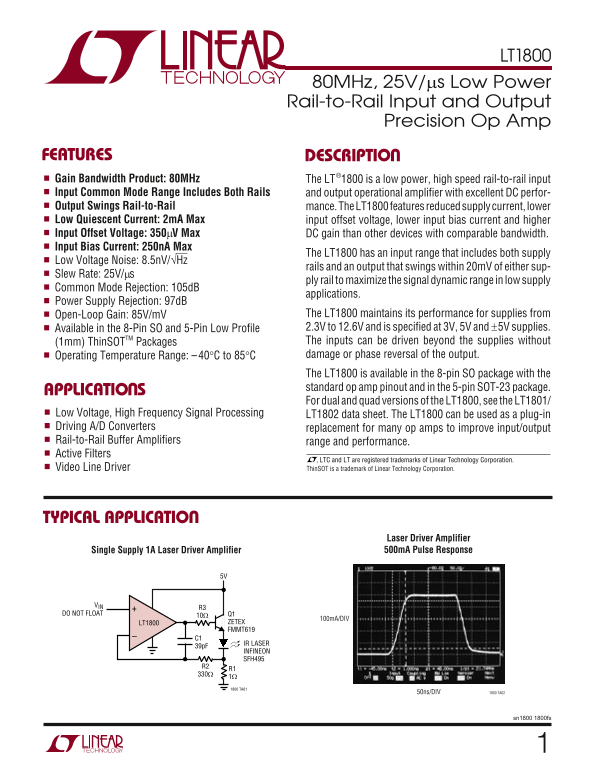
Laser Driver Amplifier Single Supply 1A Laser Driver Amplifier 500m A Pulse Response
DO NOT FLOAT Q1
100m A/DIV
LT1800 ZETEX FMMT619
IR LASER
INFINEON SFH495
1800 TA01
50ns/DIV 1800 TA02
sn1800 1800fs
Page Summary Contents For LINEAR TECHNOLOGY LT1800 sn1800 1800fs 80MHz, 25V µs Low Power Rail-to-Rail Input and Output Precision Op Amp User Manual
Manual Details
| Brand | Linear |
|---|---|
| Pages | 16 |
| File Size | 325.09 KB |
| Published | May 25, 2026 |
Enter the captcha to get the download link:

Frequently Asked Questions
What is the maximum advertised output swing for the LT1800?
The LT1800 features rail-to-rail output swings, maintaining performance from 2.3V to 12.6V and specified for 3V, 5V, and -5V supplies.
What are the primary operating constraints (temperature/package)?
The device operates across an ambient temperature range of –40°C to 85°C and is available in both 8-Pin SO and 5-Pin Low Profile SOT packages.
How does the LT1800's performance react to changes in the supply voltage?
The LT1800 maintains its overall performance characteristics (like CMRR and PSRR) across supplies ranging from 2.3V up to 12.6V, making it robust for varying power rails.