LINEAR TECHNOLOGY LT6013 LT6014 User's Manual
Summary
Discover the LT6013/LT6014, high-precision operational amplifiers engineered for demanding micro-power sensor systems. These ultra-low noise components feature exceptional rail-to-rail output swing and minimal current draw (145µA), ensuring stable operation in battery-powered applications across a wide temperature range. This manual provides comprehensive technical specifications, detailed performance data, and guidance on specialized uses, including thermocouple, photodiode, and general low-voltage interfacing. Ideal for embedded system designers requiring superior accuracy and efficiency.
Page 1 Text Content
LT6013/LT6014 Single/Dual 145µA,
9.5n V/√Hz, AV ≥5, Rail-to-Rail Output Precision Op Amps
FEATURES DESCRIPTIO 35µV Maximum Offset Voltage (LT6013A) The LT®6013 and LT6014 op amps combine low noise and Low 1/f Noise: 200n VP-P (0.1Hz to 10Hz) high precision input performance with low power con-
40n VRMS (0.1Hz to 10Hz) sumption and rail-to-rail output swing. The amplifiers are
Low White Noise: 9.5n V/√Hz (1k Hz) stable in a gain of 5 or more and feature greatly improved Rail-to-Rail Output Swing CMRR and PSRR versus frequency compared to other
145µA Supply Current per Amplifier precision op amps. 250p A Maximum Input Bias Current (LT6013A)
Input offset voltage is factory-trimmed to less than 35µV.
AV ≥5 Stable; Up to 500p F CLOAD
The low drift and excellent long-term stability ensure a
0.2V/µs Slew Rate
high accuracy over temperature and time. The 250p A
1.4MHz Gain Bandwidth Product
maximum input bias current and 120d B minimum voltage
120d B Minimum Voltage Gain, VS = ±15V
gain further maintain this precision over operating
0.8µV/°C Maximum VOS Drift
conditions.
2.7V to ±18V Supply Voltage Operation
Operating Temperature Range: –40°C to 85°C The LT6013 and LT6014 operate from any supply voltage
IN PU VO LT AG NO IS (0 .1 V/ DI V)
Available in SO-8 and Space Saving 3mm × 3mm from 2.7V to 36V and draw only 145µA of supply current DFN Packages per amplifier on a 5V supply. The output swings to within 40m V of either supply rail, making the amplifiers very APPLICATIO useful for low voltage single supply operation. Thermocouple Amplifiers The amplifiers are fully specified at 5V and ±15V supplies Precision Photodiode Amplifiers and from –40°C to 85°C. The single LT6013 and dual Instrumentation Amplifiers LT6014 are both available in SO-8 and space saving Battery-Powered Precision Systems 3mm × 3mm DFN packages. For unity gain stable ver- Low-Voltage Precision Systems sions, refer to the LT6010 and LT6011 data sheets. Micro-Power Sensor Interface , LTC and LT are registered trademarks of Linear Technology Corporation. All other trademarks are the property of their respective owners.
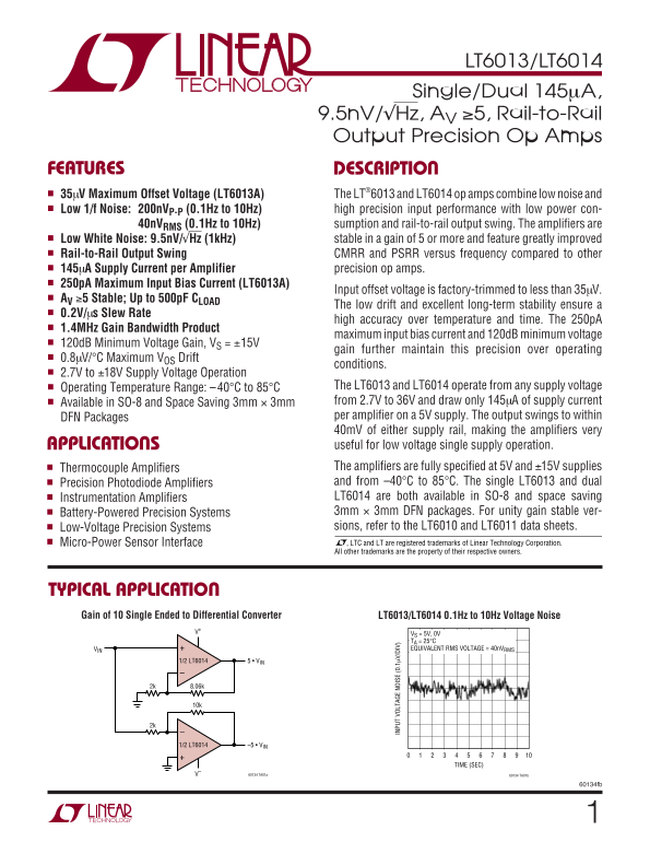
TYPICAL APPLICATIO Gain of 10 Single Ended to Differential Converter LT6013/LT6014 0.1Hz to 10Hz Voltage Noise
V+ VS = 5V, 0V
TA = 25°C VIN EQUIVALENT RMS VOLTAGE = 40n VRMS
1/2 LT6014 5 • VIN
1/2 LT6014 –5 • VIN
TIME (SEC)
V– 60134 TA01a 60134 TA01b
60134fb
Page Summary Contents For LINEAR TECHNOLOGY LT6013 LT6014 User's Manual
Manual Details
| Brand | Linear |
|---|---|
| Pages | 16 |
| File Size | 332.78 KB |
| Published | May 31, 2026 |
Enter the captcha to get the download link:

Frequently Asked Questions
What is the operating voltage range for these amplifiers?
They operate from a supply voltage of 2.7V to ±18V, or 36V total.
Can I use these low noise op amps in outdoor or variable temperature conditions?
Yes, they maintain operation within an ambient temperature range of –40°C to 85°C.
What kind of package options are available for installation on a PCB?
They are available in SO-8 and space-saving DFN packages (3mm × 3mm).
How low is the white noise output of these amplifiers?
They feature very low white noise listed at 9.5nV/√Hz.