# A B C D E F G H I J K L M N O P Q R S T U V W X Y Z

LINEAR TECHNOLOGY LT6011 LT6012 User's Manual

Summary

Designed for high-precision instrumentation, these low-power operational amplifiers provide superior performance in demanding sensing environments. Suitable for battery-powered and low voltage single supply applications, they feature exceptionally low noise, tight offset voltages, and reliable rail-to-rail output swing. This comprehensive manual details the technical specifications, thermal characteristics, various package options (DFN, SO-8, SSOP), and typical uses, making it essential documentation for circuit designers building advanced thermocouple or photo diode amplification systems.
📄 Preview PAGE OF 16

Page 1 Text Content

LT6011/LT6012

Dual/Quad135µA, 14n V/√Hz,

Rail-to-Rail Output Precision Op Amp

FEATURES DESCRIPTIO 60µV Maximum Offset Voltage The LT®6011/LT6012 op amps combine low noise and 300p A Maximum Input Bias Current high precision input performance with low power con- 135µA Supply Current per Amplifier sumption and rail-to-rail output swing. Rail-to-Rail Output Swing

Input offset voltage is trimmed to less than 60µV. The low

120d B Minimum Voltage Gain, VS = ±15V

drift and excellent long-term stability guarantee a high

0.8µV/°C Maximum VOS Drift

accuracy over temperature and time. The 300p A maxi-

14n V/√Hz Input Noise Voltage

mum input bias current and 120d B minimum voltage gain

2.7V to ±18V Supply Voltage Operation

further maintain this precision over operating conditions.

Operating Temperature Range: –40°C to 85°C

Space Saving 3mm × 3mm DFN Package The LT6011/LT6012 work on any power supply voltage from 2.7V to 36V and draw only 135µA of supply current on a 5V supply. The output swings to within 40m V of either

APPLICATIO S

supply rail, making the amplifier a good choice for low voltage single supply applications.

Thermocouple Amplifiers Precision Photo Diode Amplifiers The LT6011/LT6012 are specified at 5V and ±15V supplies Instrumentation Amplifiers and from –40°C to 85°C. The LT6011 (dual) is available in Battery-Powered Precision Systems SO-8, MS8 and space saving 3mm × 3mm DFN pack- Low Voltage Precision Systems ages. The LT6012 (quad) is available in SO-14 and 16-pin

SSOP packages. , LT, LTC and LTM are registered trademarks of Linear Technology Corporation. Soft Span is a registered trademark of Linear Technology Corporation. All other trademarks are the property of their respective owners.

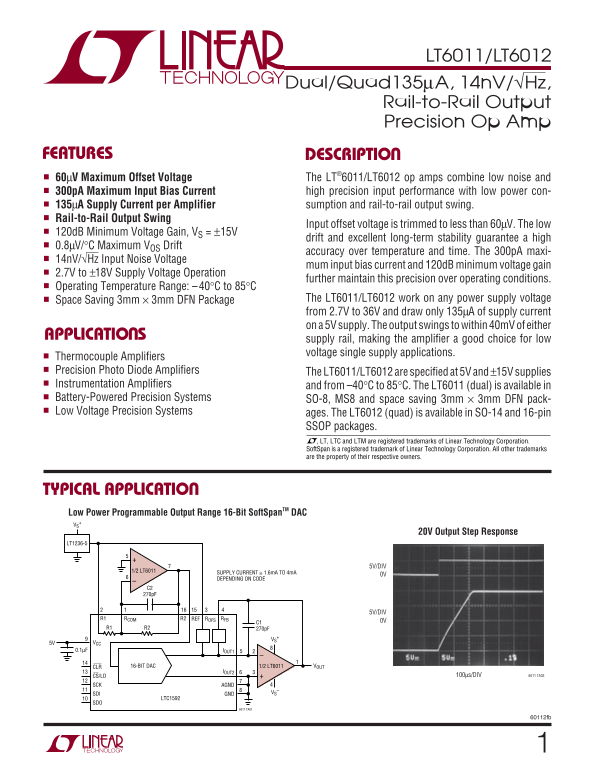
TYPICAL APPLICATIO Low Power Programmable Output Range 16-Bit Soft Span TM DAC VS

20V Output Step Response

LT1236-5

5V/DIV

1/2 LT6011 SUPPLY CURRENT ≅ 1.6m A TO 4m A

DEPENDING ON CODE

5V/DIV

R1 RCOM R2 REF ROFS RFB

5V VCC 0.1µF IOUT1

CLR 1/2 LT601116-BIT DAC VOUT

3IOUT2

CS/LD 100µs/DIV 6011 TA03

SCK AGND

SDI GND VS

LTC1592

6011 TA01

60112fb

Page Summary Contents For LINEAR TECHNOLOGY LT6011 LT6012 User's Manual

Page 1 LT6011/LT6012 Dual/Quad135µA, 14n V/√Hz, Rail-to-Rail Output Precision Op Amp FEATURES DESCRIPTIO 60µV Maximum Offset Voltage The LT®6011/LT6012 op amps combine low noise and 300p A Maximum Input Bias...
Page 2 LT6011/LT6012 (Note 1)ABSOLUTE AXI U RATI GS Total Supply Voltage (V+ to V–) 40V Maximum Junction Temperature Differential Input Voltage (Note 2) 10V DD Package 125°C Input Voltage V+ to V– All Other ...
Page 3 LT6011/LT6012 ELECTRICAL CHARACTERISTICS The ● denotes the specifications which apply over the full operating temperature range, otherwise specifications are at TA = 25°C. VS = 5V, 0V; VCM = 2.5V; RL ...
Page 4 LT6011/LT6012 ELECTRICAL CHARACTERISTICS The ● denotes the specifications which apply over the full operating temperature range, otherwise specifications are at TA = 25°C. VS = 5V, 0V; VCM = 2.5V; RL ...
Page 5 LT6011/LT6012 ELECTRICAL CHARACTERISTICS The ● denotes the specifications which apply over the full operating temperature range, otherwise specifications are at TA = 25°C. VS = ±15V, VCM = 0V, RL to 0...
Page 6 LT6011/LT6012 ELECTRICAL CHARACTERISTICS The ● denotes the specifications which apply over the full operating temperature range, otherwise specifications are at TA = 25°C. VS = ±15V, VCM = 0V, RL to 0...
Page 7 IN PU VO LT AG NO IS DE NS IT (n V/ √H z) PE RC EN OF NI TS PE RC EN OF NI TS LT6011/LT6012 TYPICAL PERFOR A CE CHARACTERISTICS Input Offset Voltage Offset Voltage Distribution of Input Offset Voltage...
Page 8 TH NO IS OU TP UT OW AT UR AT IO VO LT AG (V LT6011/LT6012 NO IS VO LT AG (0 .2 µV /D IV TYPICAL PERFOR A CE CHARACTERISTICS Output Voltage Swing Output Saturation Voltage 0.01Hz to 1Hz Noise vs Tempe...
Page 9 EN -L OO GA IN (d B) PO ER UP PL RE JE CT IO RA TI (d B) OU TP UT TE (V LT6011/LT6012 TYPICAL PERFOR A CE CHARACTERISTICS Settling Time vs Output Step Channel Separation vs Frequency CMRR vs Frequency...
Page 10 LT6011/LT6012 TYPICAL PERFOR A CE CHARACTERISTICS Small-Signal Transient Response Large-Signal Transient Response Rail-to-Rail Output Swing 20m V/DIV 2V/DIV 0V 1V/DIV AV = 1 2µs/DIV 6011 G28 AV = –1 5...
Page 11 LT6011/LT6012 APPLICATIO S I FOR ATIO where en = 14n V/√Hz , in = 0.1p A/√Hz and RS is the total Rail-to-Rail Operation impedance at the input, including the source impedance. The LT6011/LT6012 output...
Page 12 LT6011/LT6012 PACKAGE DESCRIPTIO DD Package 8-Lead Plastic DFN (3mm × 3mm) (Reference LTC DWG # 05-08-1698) (2 SIDES)2.15 ±0.05 (4 SIDES) (2 SIDES) PIN 1 TOP MARK PACKAGE (NOTE 6) OUTLINE (DD8) DFN 12...
Page 13 LT6011/LT6012 PACKAGE DESCRIPTIO MS8 Package 8-Lead Plastic MSOP (Reference LTC DWG # 05-08-1660) 0.42 ± 0.038 0.65 (.118 ± .004) 0.52 (.0165 ± .0015) (.0256) (NOTE 3) (.0205) TYP BSC REF RECOMMENDED ...
Page 14 LT6011/LT6012 PACKAGE DESCRIPTIO S14 Package 14-Lead Plastic Small Outline (Narrow .150 Inch) (Reference LTC DWG # 05-08-1610) .050 BSC NOTE 3 .228 – .244 .150 – .157 (5.791 – 6.197) (3.810 – 3.988) N...
Page 15 LT6011/LT6012 PACKAGE DESCRIPTIO GN Package 16-Lead Plastic SSOP (Narrow .150 Inch) (Reference LTC DWG # 05-08-1641) .009 (0.229) REF .254 MIN .150 – .165 .0015 .0250 BSC.0165 ± RECOMMENDED SOLDER PAD...
Page 16 LT6011/LT6012 TYPICAL APPLICATIO Low Power Hall Sensor Amplifier HALL ELEMENT ASAHI-KASEI HW-108A (RANK D) 1/2 LT6011 www.asahi-kasei.co.jp LT1790-1.25 49.9k 1, 2 OFFSET 7.87k VS 400Ω ADJUST VOUT LT17...