# A B C D E F G H I J K L M N O P Q R S T U V W X Y Z

LINEAR TECHNOLOGY LT3510 User's Manual

Summary

Achieve robust and reliable dual power conversion with this step-down switching regulator. The LT3510 provides two independent, high-efficiency 2A outputs, optimizing performance across wide input ranges (3.1V–25V). Engineered for complex systems like DSP supplies, disc drives, and modem applications, the unit offers highly synchronized tracking and low dropout performance. This technical resource covers synchronous operational modes, deep dive electrical characteristics, and integration guides necessary for reliable distributed power regulation design.
📄 Preview PAGE OF 28

Page 1 Text Content

LT3510

Monolithic Dual Tracking 2A Step-Down Switching

Regulator

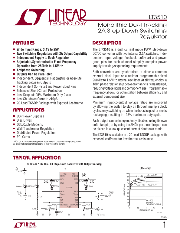
FEATURES DESCRIPTION n Wide Input Range: 3.1V to 25V The LT®3510 is a dual current mode PWM step-down n Two Switching Regulators with 2A Output Capability DC/DC converter with two internal 2.5A switches. Inde- n Independent Supply to Each Regulator pendent input voltage, feedback, soft-start and power n Adjustable/Synchronizable Fixed Frequency good pins for each channel simplify complex power Operation from 250k Hz to 1.5MHz supply tracking/sequencing requirements. n Antiphase Switching

Both converters are synchronized to either a common

n Outputs Can be Paralleled

external clock input or a resistor programmable fi xed

n Independent, Sequential, Ratiometric or Absolute

250k Hz to 1.5MHz internal oscillator. At all frequencies, a

Tracking Between Outputs

180° phase relationship between channels is maintained,

n Independent Soft-Start and Power Good Pins

reducing voltage ripple and component size. Programmable

n Enhanced Short-Circuit Protection

frequency allows for optimization between effi ciency and

n Low Dropout: 95% Maximum Duty Cycle

external component size.

n Low Shutdown Current: <10μA

n 20-Lead TSSOP Package with Exposed Leadframe Minimum input-to-output voltage ratios are improved

by allowing the switch to stay on through multiple clock

APPLICATIONS cycles, only switching off when the boost capacitor needs

recharging, resulting in ~95% maximum duty cycle.

n DSP Power Supplies

n Disc Drives

Each output can be independently disabled using its own

n DSL/Cable Modems FF IC IE

soft-start pin, or by using the SHDN pin the entire part can

n Wall Transformer Regulation

be placed in a low quiescent current shutdown mode.

n Distributed Power Regulation

The LT3510 is available in a 20-lead TSSOP package with

n PCI Cards

exposed leadframe for low thermal resistance.

, LT, LTC, and LTM are registered trademarks of Linear Technology Corporation. All other trademarks are the property of their respective owners.

TYPICAL APPLICATION 3.3V and 1.8V Dual 2A Step-Down Converter with Output Tracking VIN

Effi ciency

VIN1 VIN2 61.9k

VOUT = 3.3V

SHDN RT/SYNC VOUT = 5V

BST1 BST2

SW1 SW2

VOUT = 2.5VVOUT = 1.8V

PMEG4005 PMEG4005 B360A B360A

LT3510

VOUT1 IND1 IND2 VOUT2

3.3V VOUT1 VOUT2 1.8V 2A 47μF 100μF24.9k 2A

PG1 PG2 FB1 FB2 VIN = 12V

VC1 VC2 IOUT2 = 0A 470p F SS/TRACK1 SS/TRACK2 470p F FREQUENCY = 500k Hz

LOAD CURRENT (A)

0.1μF 3510 TA01b

TA01a

3510fc

Page Summary Contents For LINEAR TECHNOLOGY LT3510 User's Manual

Page 1 LT3510 Monolithic Dual Tracking 2A Step-Down Switching Regulator FEATURES DESCRIPTION n Wide Input Range: 3.1V to 25V The LT®3510 is a dual current mode PWM step-down n Two Switching Regulators with 2...
Page 2 LT3510 ABSOLUTE MAXIMUM RATINGS PIN CONFIGURATION (Note 1) TOP VIEW VIN1/2, SHDN, PG1/2 ...................................... 25V/–0.3V SW1/2 ............................................................
Page 3 LT3510 ELECTRICAL CHARACTERISTICS The l denotes the specifi cations which apply over the full operating temperature range, otherwise specifi cations are at TJ = 25°C. VVIN1/2 = 15V, VBST1/2 = open, VR...
Page 4 LT3510 ELECTRICAL CHARACTERISTICS LT3510IFE is guaranteed and tested over the full –40°C to 125°C operating Note 5: To enhance dropout operation, the output switch will be turned off junction temperat...
Page 5 FR k H z) (D LT3510 TYPICAL PERFORMANCE CHARACTERISTICS Soft-Start to Feedback Offset VC Switching Threshold Voltage Power Good Threshold Voltage Voltage vs Temperature vs Temperature vs Temperature R...
Page 6 VO LT AG (V TY LT3510 TYPICAL PERFORMANCE CHARACTERISTICS External Sync Duty Cycle Range Frequency and Phase vs RT/SYNC Switch Saturation Voltage vs External Sync Frequency Pin Resistance vs Switch Cu...
Page 7 LT3510 TYPICAL PERFORMANCE CHARACTERISTICS Inductor Value vs Frequency for Inductor Value vs Frequency for Dropout Operation 2A Maximum Load Current 2A Maximum Load Current LOAD = 1A VOUT = 3.3V VOUT ...
Page 8 LT3510 PIN FUNCTIONS This indicates that the output is overloaded and current is the clock signal is detected, with switch 1 in phase with pulled from the SS pin, reducing the regulation point. the sy...
Page 9 LT3510 BLOCK DIAGRAM RT/SYNC VIN ONE CHANNEL R3 OSCILLATOR INTERNAL AND REGULATOR AGC DROPOUT BST ENHANCEMENT REFERENCE SLOPE C3 COMPENSATION PRE DRIVER CIRCUITRY SHUTDOWN COMPARATOR POR UNDERVOLTAGE ...
Page 10 LT3510 APPLICATIONS INFORMATION will be generated at the incoming frequency on the rising is turned off. Once the switch is turned off the inductor edge of the synchronization pulse with switch 1 in p...
Page 11 LT3510 APPLICATIONS INFORMATION Choosing the Output Voltage The output voltage is programmed with a resistor divider FREQUENCY between the output and the FB pin. Choose the 1% resis- tors according to...
Page 12 LT3510 APPLICATIONS INFORMATION maximum duty cycle. The duty cycle is the fraction of time VOUT = 3.3V that the internal switch is on during a clock cycle. Unlike most fi xed frequency regulators, the...
Page 13 LT3510 APPLICATIONS INFORMATION and its saturation current should be about 30% higher. To 2.5A over the entire duty cycle range. The maximum output keep effi ciency high, the series resistance (DCR) s...
Page 14 LT3510 APPLICATIONS INFORMATION may result in discontinuous mode operation, which is ments of the input capacitor. Determine the worst-case okay, but further reduces maximum load current. For conditio...
Page 15 LT3510 APPLICATIONS INFORMATION either clamp the input voltage or dampen the tank circuit The RMS content of this ripple is very low, and the RMS by adding a lossy capacitor in parallel with the ceram...
Page 16 LT3510 APPLICATIONS INFORMATION Table 2 where IOUT(MAX) is the maximum load current, and VBST(MIN) is the minimum boost voltage to fully saturate VENDOR TYPE SERIES the switch. Taiyo Yuden Ceramic X5R...
Page 17 LT3510 APPLICATIONS INFORMATION BST BST VINVIN SW VINVIN SW LT3510 LT3510 IND IND VOUT VOUT VOUT VOUT &lt; 3V GND GND VBST – VSW = VOUT VBST – VSW = VIN VBST(MAX) = VIN + VOUT VBST(MAX) = 2 • VIN VX =...
Page 18 LT3510 APPLICATIONS INFORMATION LT3510 CURRENT MODE SW POWER STAGE OUTPUT gm = 2.2mho R1 CPL ESR gm = 275μmho RC 3.6M CERAMIC ERROR TANTALUM AMP 0.8V R2 CF OR POLYMER Figure 6. Model for Loop Response...
Page 19 LT3510 APPLICATIONS INFORMATION If the synchronization signal powers up in a high impedance defaults the open-pin condition to be operating (see Typical state (Hi-Z), connect a resistor from the RT/SY...
Page 20 LT3510 APPLICATIONS INFORMATION At power-up, a reset signal sets the soft-start latch and threshold is exceeded. The PG pin is active (sink capability discharges both SS pins to approximately 0V to en...
Page 21 LT3510 APPLICATIONS INFORMATION Independent Start-Up Ratiometric Start-Up Absolute Start-Up VOUT1 VOUT1 VOUT1 0.5V/DIV 0.5V/DIV 0.5V/DIV PG1 PG1PG1 VOUT2 VOUT2 VOUT2 0.5V/DIV 0.5V/DIV 0.5V/DIV PG2 PG2...
Page 22 LT3510 APPLICATIONS INFORMATION VIN 6V TO 24V PMEG4005 VIN1 VIN2 26.7k SHDN FSET BST1 BST2 SW1 SW2 PMEG4005 B360A B360A LT3510 IND1 IND2 VOUT1 VOUT2 VOUT1 VOUT2 PG1 PG2 FB1 FB2 VC1 VC2 8.06k SS/TRACK1...
Page 23 LT3510 APPLICATIONS INFORMATION VIN LT3510 LT3510 VIN LT3510 SW SW SWVIN GND GND GND Figure 11. Subtracting the Current when the Switch is On (11a) from the Current when the Switch is Off (11b) Reveal...
Page 24 LT3510 APPLICATIONS INFORMATION to the internal planes with vias can further reduce ther- There is one special consideration regarding the 2-phase mal resistance. With these steps, the thermal resista...
Page 25 LT3510 TYPICAL APPLICATIONS 5V and 2.5V with Absolute Tracking VIN 12V VIN1 VIN2 26.7k SHDN RT/SYNC BST1 BST2 SW1 SW2 B360A B360A PMEG4005 PMEG4005 LT3510 IND1 IND2 VOUT1 VOUT2 VOUT1 VOUT2 PG1 PG2 FB1...
Page 26 LT3510 TYPICAL APPLICATIONS 1.25MHz Single 3.3V/4A Low Ripple Output VIN 4.5V TO 6V VIN1 VIN2 SHDN RT/SYNC PMEG4005* PMEG4005* BST1 BST2 SW1 SW2 B360A B360A PMEG4005PMEG4005 LT3510 VOUT1 IND1 IND2 3.3...
Page 27 LT3510 PACKAGE DESCRIPTION FE Package 20-Lead Plastic TSSOP (4.4mm) (Reference LTC DWG # 05-08-1663) Exposed Pad Variation CA SEE NOTE 4 (.252) (.108) BSC 0.65 BSC RECOMMENDED SOLDER PAD LAYOUT 0.25 M...
Page 28 LT3510 RELATED PARTS PART NUMBER DESCRIPTION COMMENTS LT1766 60V, 1.2A (IOUT), 200k Hz High Effi ciency Step-Down DC/DC VIN: 5.5V to 60V, VOUT(MIN) = 1.20V, IQ = 2.5m A, ISD = 25μA, Converter 16-Lead ...

Manual Details

Brand Linear
Pages 28
File Size 306.18 KB
Published June 16, 2026
2 views

Enter the captcha to get the download link:

captcha

Frequently Asked Questions

What is the maximum output capability of each regulator?

Each dual current mode PWM step-down converter has a 2A output capability.

How do the two converters maintain synchronization?

They maintain an 180° phase relationship (antiphase switching) at all operating frequencies.

What is the span of the adjustable operating frequency?

The internal oscillator allows for operation at frequencies ranging from 250kHz to 1.5MHz.

How can I manage individual outputs during low power states?

Each output can be independently managed using its own SHDN pin or Power Good (PG) pin.

What range of input voltages does the LT3510 support?

The product supports a wide input voltage range from 3.1V to 25V.