# A B C D E F G H I J K L M N O P Q R S T U V W X Y Z

LINEAR TECHNOLOGY LT1991 High Precision, Selectable Gain Amplifier Data Sheet Owner's Manual

Summary

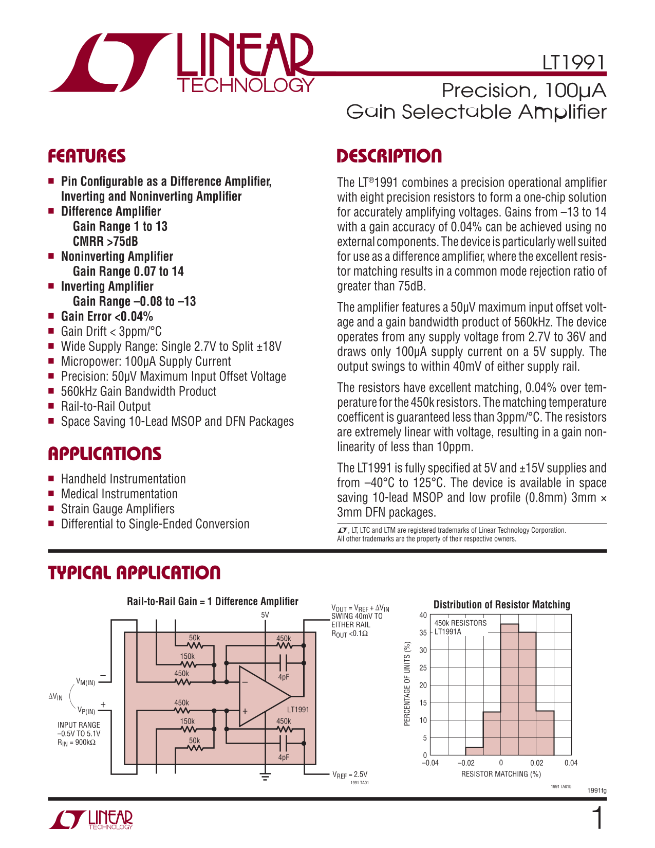
The LT1991 is a highly precise, low-power gain-selectable differential amplifier designed for demanding applications like medical instrumentation and strain gauge measurement. Integrating eight precision resistors, it offers excellent common mode rejection (CMRR >75dB) and operates across a wide supply range (2.7V to 36V). This technical resource provides detailed specifications, typical circuit examples, thermal data, and package information, making it essential for engineers implementing high-accuracy signal conditioning in handheld or industrial devices.
📄 Preview PAGE OF 28

Page 1 Text Content

LT1991

Precision, 100µA

Gain Selectable Amplifi er

FEATURES DESCRIPTION n Pin Confi gurable as a Difference Amplifi er,

The LT®1991 combines a precision operational amplifi er

Inverting and Noninverting Amplifi er with eight precision resistors to form a one-chip solution n Difference Amplifi er for accurately amplifying voltages. Gains from –13 to 14 Gain Range 1 to 13 with a gain accuracy of 0.04% can be achieved using no CMRR >75d B external components. The device is particularly well suited n Noninverting Amplifi er for use as a difference amplifi er, where the excellent resis-

Gain Range 0.07 to 14 tor matching results in a common mode rejection ratio of

n Inverting Amplifi er greater than 75d B. Gain Range –0.08 to –13

The amplifi er features a 50μV maximum input offset volt-

n Gain Error <0.04%

age and a gain bandwidth product of 560k Hz. The device

n Gain Drift < 3ppm/°C

operates from any supply voltage from 2.7V to 36V and

n Wide Supply Range: Single 2.7V to Split ±18V

draws only 100μA supply current on a 5V supply. The

n Micropower: 100μA Supply Current

output swings to within 40m V of either supply rail.

n Precision: 50μV Maximum Input Offset Voltage

n 560k Hz Gain Bandwidth Product The resistors have excellent matching, 0.04% over tem- n Rail-to-Rail Output perature for the 450k resistors. The matching temperature

TA IT

coeffi cent is guaranteed less than 3ppm/°C. The resistors

n Space Saving 10-Lead MSOP and DFN Packages

are extremely linear with voltage, resulting in a gain non- linearity of less than 10ppm.

APPLICATIONS

The LT1991 is fully specifi ed at 5V and ±15V supplies and

n Handheld Instrumentation

from –40°C to 125°C. The device is available in space

n Medical Instrumentation

saving 10-lead MSOP and low profi le (0.8mm) 3mm ×

n Strain Gauge Amplifi ers

3mm DFN packages.

n Differential to Single-Ended Conversion

L, LT, LTC and LTM are registered trademarks of Linear Technology Corporation. All other trademarks are the property of their respective owners.

TYPICAL APPLICATION

Rail-to-Rail Gain = 1 Difference Amplifi er

VOUT = VREF ΔVIN Distribution of Resistor Matching

5V SWING 40m V TO

EITHER RAIL 450k RESISTORS ROUT <0.1Ω LT1991A

VM(IN)

VP(IN) LT1991

INPUT RANGE –0.5V TO 5.1V

RIN = 900kΩ 50k

VREF = 2.5V RESISTOR MATCHING (%)

1991 TA01

1991 TA01b

1991fg

Page Summary Contents For LINEAR TECHNOLOGY LT1991 High Precision, Selectable Gain Amplifier Data Sheet Owner's Manual

Page 1 LT1991 Precision, 100µA Gain Selectable Amplifi er FEATURES DESCRIPTION n Pin Confi gurable as a Difference Amplifi er, The LT®1991 combines a precision operational amplifi er Inverting and Noninverti...
Page 2 LT1991 ABSOLUTE MAXIMUM RATINGS (Note 1) Specifi ed Temperature Range (Note 5) Total Supply Voltage (V+ to V–) ................................40V LT1991C ................................................
Page 3 LT1991 ELECTRICAL CHARACTERISTICS The l denotes the specifi cations which apply over the operating temperature range of 0°C to 70°C for C-grade parts and –40°C to 85°C for I-grade parts, otherwise spe...
Page 4 LT1991 ELECTRICAL CHARACTERISTICS The l denotes the specifi cations which apply over the operating temperature range of 0°C to 70°C for C-grade parts and –40°C to 85°C for I-grade parts, otherwise spe...
Page 5 LT1991 ELECTRICAL CHARACTERISTICS The l denotes the specifi cations which apply over the operating temperature range of –40°C to 125°C for H-grade parts, otherwise specifi cations are at TA = 25°C. Di...
Page 6 LT1991 ELECTRICAL CHARACTERISTICS The l denotes the specifi cations which apply over the operating temperature range of –40°C to 125°C for H-grade parts, otherwise specifi cations are at TA = 25°C. Di...
Page 7 TP FF ET LT (µ LY LT1991 TYPICAL PERFORMANCE CHARACTERISTICS (Difference Amplifi er Confi guration) Output Voltage Swing Output Voltage Swing Supply Current vs Supply Voltage vs Temperature vs Load Cu...
Page 8 IN ID k H z) LT1991 TYPICAL PERFORMANCE CHARACTERISTICS (Difference Amplifi er Confi guration) Bandwidth vs Gain CMRR vs Frequency PSRR vs Frequency VS = 5V, 0V VS = 5V, 0V VS = 5V, 0V TA = 25°C TA = ...
Page 9 LT1991 TYPICAL PERFORMANCE CHARACTERISTICS Small Signal Transient Response Small Signal Transient Response Small Signal Transient Response GAIN = 1 GAIN = 3 GAIN = 9 50m V/DIV 50m V/DIV 50m V/DIV 5μs/...
Page 10 LT1991 APPLICATIONS INFORMATION Introduction admittances. Because it has 9 times the admittance, the voltage applied to the P9 input has 9 times the effect of The LT1991 may be the last op amp you eve...
Page 11 LT1991 APPLICATIONS INFORMATION The maximum voltage allowed on the P3, M3, P9, and as a gain of 13 difference amplifi er on a single supply M9 inputs includes the positive and negative supply plus wit...
Page 12 LT1991 APPLICATIONS INFORMATION with VMORE = 0, the op amp output is at VREF. From the representation of the circuit on the top. The LT1991 is max VEXT (the high cm limit), as VMORE goes positive, the...
Page 13 LT1991 APPLICATIONS INFORMATION Table 1. Confi guring the M Pins for Simple Noninverting Gains. The P Inputs are driven as shown in the examples on the next page. M9, M3, M1 Connection Gain M9 M3 M1 O...
Page 14 LT1991 APPLICATIONS INFORMATION VS VS VS VCC VCC VCC M1 M1 M1 LT1991 OUT VOUT LT1991 OUT VOUT LT1991 OUT VOUT P1 REF VIN P1 REF P1 REF P3 VEE P3 VEE P3 VEE VIN P9 P9 VIN P9 VS VS GAIN = 1 GAIN = 2 GAI...
Page 15 LT1991 APPLICATIONS INFORMATION Attenuation Using the P Input Resistors Table 2. Confi guring the P Pins for Various Attenuations. Those Shown in Bold Are Functional Even When the Input Drive Attenuat...
Page 16 LT1991 APPLICATIONS INFORMATION Inverting Confi guration Table 3. Confi guring the M Pins for Simple Inverting Gains M9, M3, M1 Connection The inverting amplifi er, shown in Figure 8, is another class...
Page 17 LT1991 APPLICATIONS INFORMATION VS VS VS M9 M9 VIN M9 VCC VCC VCC VIN M1 VIN M1 M1 LT1991 OUT VOUT LT1991 OUT VOUT LT1991 OUT VOUT P1 REF P1 REF P1 REF P3 VEE P3 VEE P3 VEE P9 P9 P9 VS VS GAIN = –0.25...
Page 18 LT1991 APPLICATIONS INFORMATION Difference Amplifi ers RF The resistors in the LT1991 allow it to easily make differ- ence amplifi ers also. Figure 10 shows the basic 4-resistor RG VIN difference ampl...
Page 19 LT1991 APPLICATIONS INFORMATION VS VS VS M9 M9 VIN M9 VCC VCC VCC VIN M1 VIN M1 M1 LT1991 OUT VOUT LT1991 OUT VOUT LT1991 OUT VOUT VIN P1 REF VIN P1 REF P1 REF P3 VEE P3 VEE P3 VEE P9 P9 VIN P9 VS VS ...
Page 20 LT1991 APPLICATIONS INFORMATION CROSS- COUPLING VOUT RG 450k VOUT 150k 4p F RG P3 VOUT = GAIN • (VIN – VIN RF GAIN = RF/RG 50k 450k P9 LT1991 CLASSICAL DIFFERENCE AMPLIFIER IMPLEMENTED CLASSICAL DIFFE...
Page 21 LT1991 APPLICATIONS INFORMATION High Voltage CM Difference Amplifi ers Table 6. High V CM Connections Giving Difference Gains for the LT1991 This class of difference amplifi er remains to be discussed...
Page 22 LT1991 APPLICATIONS INFORMATION VCC VCC VCC VIN M1 VIN M1 VIN M1 LT1991 OUT VOUT LT1991 OUT VOUT LT1991 OUT VOUT VIN P1 REF VIN P1 REF VIN P1 REF P3 VEE P3 VEE P3 VEE VCM = 0.8V TO 2.35V VCM = 2V TO 3...
Page 23 LT1991 APPLICATIONS INFORMATION VCC VCC VCC VIN M1 VIN M1 VIN M1 LT1991 OUT VOUT LT1991 OUT VOUT LT1991 OUT VOUT VIN P1 REF VIN P1 REF VIN P1 REF P3 VEE P3 VEE P3 VEE VCM = –0.5V TO 5.1V VCM = 2V TO 7...
Page 24 LT1991 APPLICATIONS INFORMATION VCC VCC VCC VIN M1 VIN M1 VIN M1 LT1991 OUT VOUT LT1991 OUT VOUT LT1991 OUT VOUT VIN P1 REF VIN P1 REF VIN P1 REF P3 VEE P3 VEE P3 VEE P9 P9 P9 –5V –5V –5V VCM = –8V TO...
Page 25 LT1991 TYPICAL APPLICATIONS Micropower AV = 10 Instrumentation Amplifi er 1/2 LT6011 LT1991 VP 1/2 LT6011 1991 TA02 1991fg
Page 26 LT1991 PACKAGE DESCRIPTION DD Package 10-Lead Plastic DFN (3mm × 3mm) (Reference LTC DWG # 05-08-1699) (2 SIDES)2.15 ±0.05 PACKAGE OUTLINE 0.50 BSC 2.38 ±0.05 (2 SIDES) RECOMMENDED SOLDER PAD PITCH AN...
Page 27 LT1991 PACKAGE DESCRIPTION MS Package 10-Lead Plastic MSOP (Reference LTC DWG # 05-08-1661) (NOTE 3) (.0120 ± .0015) (.0197) (.0196 ± .003) TYP BSC REF RECOMMENDED SOLDER PAD LAYOUT DETAIL “A” (.118 ±...
Page 28 LT1991 TYPICAL APPLICATION Bidirectional Current Source Single Supply AC Coupled Amplifi er VS = 2.7V TO 36VVS VIN M1 M1 LT1991 VOUTLT1991 VIN P1 R1 VCC P1 R2* 10k 0.1μF P9 VIN P9 VIN + – VIN ILOAD = ...

Manual Details

Brand Linear
Pages 28
File Size 290.26 KB
Published June 22, 2026
5 views

Enter the captcha to get the download link:

captcha

Frequently Asked Questions

What is the operational gain range of the LT1991 amplifier?

The device supports a wide gain range from –13 to 14.

How efficient is the LT1991 in terms of power consumption?

It features micropower operation, drawing only 100µA supply current on a 5V supply.

What temperature extremes can the LT1991 handle?

Operating ranges vary by model; the LT1991H version supports –40°C to 125°C operation and storage.

Is this device suitable for space-constrained designs?

Yes, it is available in small 10-Lead MSOP and DFN packages.