# A B C D E F G H I J K L M N O P Q R S T U V W X Y Z

LINEAR TECHNOLOGY LT1956 LT1956-5 Specifications User Guide

Summary

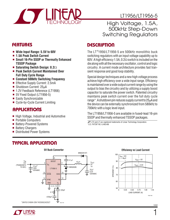
The LT1956 series are high-efficiency, 1.5A step-down switching regulators designed for demanding applications requiring stable power from wide input voltages (up to 60V). Featuring advanced current mode control, these robust converters maintain peak performance and efficiency across a full duty cycle range. This manual provides comprehensive technical specifications, operational guidelines, detailed application circuits, and packaging information needed for integration into portable computers, battery chargers, and distributed industrial/automotive power systems.
📄 Preview PAGE OF 28

Page 1 Text Content

LT1956/LT1956-5 High Voltage, 1.5A, 500k Hz Step-Down Switching Regulators

FEATURES DESCRIPTIO

®1956/LT1956-5 are 500k Hz monolithic buck

Wide Input Range: 5.5V to 60V The LT 1.5A Peak Switch Current switching regulators with an input voltage capability up to Small 16-Pin SSOP or Thermally Enhanced 60V. A high efficiency 1.5A, 0.2Ω switch is included on the

TSSOP Package die along with all the necessary oscillator, control and logic

Saturating Switch Design: 0.2Ω circuitry. A current mode architecture provides fast tran- Peak Switch Current Maintained Over sient response and good loop stability. Full Duty Cycle Range

Special design techniques and a new high voltage process

Constant 500k Hz Switching Frequency

achieve high efficiency over a wide input range. Efficiency

Effective Supply Current: 2.5m A

is maintained over a wide output current range by using the

Shutdown Current: 25µA

output to bias the circuitry and by utilizing a supply boost

1.2V Feedback Reference (LT1956)

capacitor to saturate the power switch. Patented circuitry

5V Fixed Output (LT1956-5)

maintains peak switch current over the full duty cycle

Easily Synchronizable

range*. A shutdown pin reduces supply current to 25µA and

Cycle-by-Cycle Current Limiting

the device can be externally synchronized from 580k Hz to 700k Hz with a logic level input.

APPLICATIO S

EF FI CI EN CY

The LT1956/LT1956-5 are available in fused-lead 16-pin

High Voltage, Industrial and Automotive

SSOP and thermally enhanced TSSOP packages.■

Portable Computers

, LTC and LT are registered trademarks of Linear Technology Corporation. Battery-Powered Systems *U.S. PATENT NO. 6,498,466

Battery Chargers Distributed Power Systems

TYPICAL APPLICATIO

5V Buck Converter Efficiency vs Load Current

MMSD914TI

VIN = 12V L = 18µH

VOUT = 5V

VIN BOOST

10µH VOUT

VIN SW 5V

(TRANSIENTS VOUT = 3.3V

TO 60V) 10MQ060N

100V LT1956-5

CERAMIC

6.3V SHDN BIAS CERAMIC

SYNC FB

VCGND

4.7k LOAD CURRENT (A)

1956 TA02

†UNITED CHEMI-CON THCS50EZA225ZT

1956 TA01

Page Summary Contents For LINEAR TECHNOLOGY LT1956 LT1956-5 Specifications User Guide

Page 1 LT1956/LT1956-5 High Voltage, 1.5A, 500k Hz Step-Down Switching Regulators FEATURES DESCRIPTIO ®1956/LT1956-5 are 500k Hz monolithic buck Wide Input Range: 5.5V to 60V The LT 1.5A Peak Switch Current ...
Page 2 LT1956/LT1956-5 ABSOLUTE AXI U RATI GS (Note 1) Input Voltage (VIN) 60V Operating Junction Temperature Range BOOST Pin Above SW 35V LT1956EFE/LT1956EFE-5/LT1956EGN/LT1956EGN-5 BOOST Pin Voltage 68V (N...
Page 3 LT1956/LT1956-5 ELECTRICAL CHARACTERISTICS The ● denotes specifications which apply over the full operating temperature range, otherwise specifications are at TJ = 25°C. VIN = 15V, VC = 1.5V, SHDN = 1...
Page 4 TR AN SC ON DU CT AN CE (µ ho SH DN IN OL TA GE (V SW IT CH EA CU RR EN (A LT1956/LT1956-5 TYPICAL PERFOR A CE CHARACTERISTICS Switch Peak Current Limit FB Pin Voltage and Current SHDN Pin Bias Curren...
Page 5 TH RE SH OL VO LT AG (V FR EQ UE NC (k Hz LT1956/LT1956-5 TYPICAL PERFOR A CE CHARACTERISTICS Minimum Input Voltage with 5V Switching Frequency Output BOOST Pin Current 7.5 VOUT = 5V L = 18µH 7.0 MINI...
Page 6 LT1956/LT1956-5 PI FU CTIO S GND (Pins 1, 8, 9, 16): The GND pin connections act as VC (Pin 11) The VC pin is the output of the error amplifier the reference for the regulated output, so load regulati...
Page 7 LT1956/LT1956-5 BLOCK DIAGRA The LT1956 is a constant frequency, current mode buck it much easier to frequency compensate the feedback loop converter. This means that there is an internal clock and an...
Page 8 LT1956/LT1956-5 APPLICATIO S I FOR ATIO FEEDBACK PIN FUNCTIONS current through the diode and inductor is equal to the short-circuit current limit of the switch (typically 2A for The feedback (FB) pin ...
Page 9 LT1956/LT1956-5 APPLICATIO S I FOR ATIO LT1956 VSW L1 TO FREQUENCY OUTPUT SHIFTING ERROR AMPLIFIER 2k FB BUFFER TO SYNC CIRCUIT VC GND Figure 2. Frequency and Current Limit Foldback with high input vo...
Page 10 LT1956/LT1956-5 APPLICATIO S I FOR ATIO Peak-to-peak output ripple voltage is the sum of a triwave ceramic capacitor. Although this reduction of ESR re- (created by peak-to-peak ripple current (ILP-P)...
Page 11 LT1956/LT1956-5 APPLICATIO S I FOR ATIO iron cores are forgiving because they saturate softly, current without affecting the frequency compensation it whereas ferrite cores saturate abruptly. Other co...
Page 12 LT1956/LT1956-5 APPLICATIO S I FOR ATIO solution. The maximum output load current in discontinu- load current is required, the inductor value must be ous mode, however, must be calculated and is defin...
Page 13 LT1956/LT1956-5 APPLICATIO S I FOR ATIO where: capacitor may potentially be starting from 0V. This re- quires that the part obey the overall duty cycle demanded f = switching frequency by the loop, re...
Page 14 LT1956/LT1956-5 APPLICATIO S I FOR ATIO Output capacitor ripple current (RMS): is to prevent excessive ripple causing dips below the mini- mum operating voltage resulting in erratic operation. OUT IN ...
Page 15 LT1956/LT1956-5 APPLICATIO S I FOR ATIO internal switch will ramp up VIN current into the diode in an A 0.1µF boost capacitor is recommended for most appli- attempt to get it to recover. Then, when th...
Page 16 LT1956/LT1956-5 APPLICATIO S I FOR ATIO LT1956 L1 VSW OUTPUT INPUT IN 2.38V STANDBY TOTAL SHUTDOWN RLOC2 0.4V Figure 4. Undervoltage Lockout bypassed with a 1000p F capacitor to prevent coupling SYNCH...
Page 17 LT1956/LT1956-5 APPLICATIO S I FOR ATIO LAYOUT CONSIDERATIONS LT1956 As with all high frequency switchers, when considering layout, care must be taken in order to achieve optimal electrical, thermal a...
Page 18 LT1956/LT1956-5 APPLICATIO S I FOR ATIO Board layout also has a significant effect on thermal resis- a >100MHz oscilloscope must be used, and waveforms tance. For the GN package, Pins 1, 8, 9 and 1...
Page 19 LT1956/LT1956-5 APPLICATIO S I FOR ATIO Boost current loss: IN OUT LOAD VDIODE IN OUT OUT VBOOST VF = Forward voltage of diode (assume 0.63V at 1A) Quiescent current loss: WDIODE VQ 003. )0 IN OUT= No...
Page 20 LT1956/LT1956-5 APPLICATIO S I FOR ATIO Note: Some of the internal power dissipation in the IC, due A zener, D4, placed in series with D2 (see Figure 9), drops to BOOST pin voltage, can be transferred...
Page 21 LT1956/LT1956-5 APPLICATIO S I FOR ATIO Input Voltage vs Operating Frequency Considerations circuits, read the Layout Considerations section first. Common layout errors that appear as stability proble...
Page 22 PHASE (DEG) LT1956/LT1956-5 APPLICATIO S I FOR ATIO LT1956 CURRENT MODE SW OUTPUT GAIN POWER STAGE gm = 2mho ERROR AMPLIFIER CFB R1 FB TANTALUM CERAMIC gm = 2000µmho ESR PHASE RO 1.22V RLOAD GND VC –2...
Page 23 LT1956/LT1956-5 APPLICATIO S I FOR ATIO MMSD914TI 10MQ060N BOOST REMOVABLE VIN LT1956 SW INPUT R3 5V, 1A ALTERNATE 54k SUPPLY SYNC FB VCGND 100µF 10MQ060N 4.99k RC CF CC 0.022µF Figure 12. Dual Source...
Page 24 UT AX IM UM OA CU RR EN (m A) LT1956/LT1956-5 APPLICATIO S I FOR ATIO D2 MMSD914TI VIN BOOST 9V TO 12V VOUT1** VIN SW (TRANSIENTS 5V LT1956 TO 36V) SHDN R1 C3 15.4k C5 2.2µF SYNC FB 10µF 50V 6.3V VCGN...
Page 25 LT1956/LT1956-5 APPLICATIO S I FOR ATIO current in L2 and C4 flows via the catch diode D3, charging IN OUT the negative output capacitor C6. If the negative output is OUT IN OUT IN not loaded enough, ...
Page 26 LT1956/LT1956-5 PACKAGE DESCRIPTIO Minimum inductor continuous mode: The output capacitor ripple current for the positive-to- negative converter is similar to that for a typical buck IN OUT regulator—...
Page 27 LT1956/LT1956-5 PACKAGE DESCRIPTIO FE Package 16-Lead Plastic TSSOP (4.4mm) (Reference LTC DWG # 05-08-1663) Exposed Pad Variation BB SEE NOTE 4 2.94 6.40 (.116) BSC 0.65 BSC 2RECOMMENDED SOLDER PAD L...
Page 28 LT1956/LT1956-5 PACKAGE DESCRIPTIO GN Package 16-Lead Plastic SSOP (Narrow .150 Inch) (Reference LTC DWG # 05-08-1641) .009 (0.229) REF .254 MIN .150 – .165 .0015 .0250 TYP.0165 ± RECOMMENDED SOLDER P...

Manual Details

Brand Linear
Pages 28
File Size 304.52 KB
Published June 19, 2026
6 views

Enter the captcha to get the download link:

captcha

Frequently Asked Questions

What is the input voltage range for this regulator?

The LT1956/LT1956-5 supports a wide input range from 5.5V to 60V.

Do these regulators support external synchronization?

Yes, the device can be externally synchronized with a logic level input ranging from 580kHz to 700kHz.

What is the shutdown current of the LT1956-5?

The shutdown pin reduces supply current down to 25mA.