# A B C D E F G H I J K L M N O P Q R S T U V W X Y Z

LINEAR TECHNOLOGY LT1766 LT1766-5 Specifications User Guide

Summary

This datasheet describes the Linear Technology LT1766 and LT1766-5 monolithic buck switching regulators accepting 5.5V to 60V input with an integrated 1.5A peak switch rated at 0.2Ω. Operating at a constant 200kHz switching frequency with current mode control for fast transient response, the devices maintain peak switch current over the full duty cycle range using patented circuitry. The LT1766 provides a 1.2V feedback reference for adjustable output, while the LT1766-5 delivers a fixed 5V outpu
📄 Preview PAGE OF 28

Page 1 Text Content

LT1766/LT1766-5

5.5V to 60V 1.5A, 200k Hz Step-Down Switching Regulator

FEATURES DESCRIPTIO

®1766/LT1766-5 are 200k Hz monolithic buck

Wide Input Range: 5.5V to 60V The LT 1.5A Peak Switch Current switching regulators that accept input voltages up to 60V.

Constant 200k Hz Switching Frequency A high efficiency 1.5A, 0.2Ω switch is included on the die

Saturating Switch Design: 0.2Ω along with all the necessary oscillator, control and logic cir- Peak Switch Current Rating Maintained Over cuitry. A current mode control architecture delivers fast

Full Duty Cycle Range transient response and excellent loop stability.

Low Effective Supply Current: 2.5m A

Special design techniques and a new high voltage process

Low Shutdown Current: 25µA

achieve high efficiency over a wide input range. Efficiency

1.2V Feedback Reference Voltage (LT1766)

is maintained over a wide output current range by using the

5V Fixed Output (LT1766-5)

output to bias the circuitry and by utilizing a supply boost

Easily Synchronizable

capacitor to saturate the power switch. Patented circuitry*

Cycle-by-Cycle Current Limiting

maintains peak switch current over the full duty cycle range.

Small 16-Pin SSOP and Thermally Enhanced

A shutdown pin reduces supply current to 25µA and the

TSSOP Packages

device can be externally synchronized from 228k Hz to 700k Hz with logic level inputs.

APPLICATIO S

The LT1766/LT1766-5 are available in a 16-pin fused-lead

High Voltage, Industrial and Automotive

SSOP package or a TSSOP package with exposed backside

EF FI CI EN CY

Portable Computers

for improved thermal performance.

Battery-Powered Systems

, LTC and LT are registered trademarks of Linear Technology Corporation. All other

Battery Chargers trademarks are the property of their respective owners. *Protected by U.S. Patents

including 6498466, 6531909

Distributed Power Systems

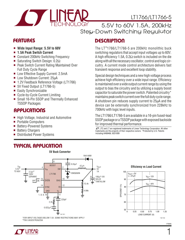
TYPICAL APPLICATIO

5V Buck Converter

BOOST 47µH

VIN VOUT Efficiency vs Load Current 5.5V* VIN SW 5V TO 60V 2.2µF† 1A

10MQ060N VOUT = 5V

100V LT1766

L = 47µH VIN = 12V

CERAMIC 100µF 10V

SOLID

ONOFF SHDN BIAS

TANTALUM

15.4k VIN = 42V

SYNC FB

VCGND 4.99k

1766 TA01 LOAD CURRENT (A)

FOR INPUT VOLTAGES BELOW 7.5V, SOME RESTRICTIONS MAY APPLY 1766 TA02

TDK C4532X7R2A225K

1766fb

Page Summary Contents For LINEAR TECHNOLOGY LT1766 LT1766-5 Specifications User Guide

Page 1 LT1766/LT1766-5 5.5V to 60V 1.5A, 200k Hz Step-Down Switching Regulator FEATURES DESCRIPTIO ®1766/LT1766-5 are 200k Hz monolithic buck Wide Input Range: 5.5V to 60V The LT 1.5A Peak Switch Current swi...
Page 2 LT1766/LT1766-5 ABSOLUTE AXI U RATI GS (Note 1) Input Voltage (VIN) 60V Operating Junction Temperature Range BOOST Pin Above SW 35V LT1766EFE/LT1766EFE-5/LT1766EGN/ BOOST Pin Voltage 68V LT1766EGN-5 (...
Page 3 LT1766/LT1766-5 ELECTRICAL CHARACTERISTICS (LT1766E/LT1766I GRADE) The ● denotes specifications which apply over the full operating temperature range, otherwise specifications are at TJ = 25°C. VIN = ...
Page 4 LT1766/LT1766-5 ELECTRICAL CHARACTERISTICS (LT1766H GRADE) The ● denotes specifications which apply over the full operating temperature range, otherwise specifications are at TJ = 25°C. VIN = 15V, VC ...
Page 5 TR AN SC ON DU CT AN CE (µ ho SH DN IN OL TA GE (V SW IT CH EA CU RR EN (A LT1766/LT1766-5 TYPICAL PERFOR A CE CHARACTERISTICS Switch Peak Current Limit FB Pin Voltage and Current SHDN Pin Bias Curren...
Page 6 TH RE SH OL VO LT AG (V FR EQ UE NC (k Hz LT1766/LT1766-5 TYPICAL PERFOR A CE CHARACTERISTICS Minimum Input Voltage with 5V Switching Frequency Output BOOST Pin Current 7.5 TA = 25°C TA = 25°C MINIMUM...
Page 7 LT1766/LT1766-5 PI FU CTIO S VIN (Pin 4): This is the collector of the on-chip power NPN FB/SENSE (Pin 12): The feedback pin is used to set the switch. VIN powers the internal control circuitry when a...
Page 8 LT1766/LT1766-5 BLOCK DIAGRA The current fed system will have 90° phase shift at a much regulated output voltage). This will improve efficiency if lower frequency, but will not have the additional 90°...
Page 9 LT1766/LT1766-5 APPLICATIO S I FOR ATIO FEEDBACK PIN FUNCTIONS switching regulator to operate at very low duty cycles, and the average current through the diode and inductor The feedback (FB) pin on t...
Page 10 LT1766/LT1766-5 APPLICATIO S I FOR ATIO LT1766 VSW TO FREQUENCY L1 OUTPUT SHIFTING ERROR AMPLIFIER 2k FB BUFFER TO SYNC CIRCUIT VC GND Figure 2. Frequency and Current Limit Foldback should be used if ...
Page 11 LT1766/LT1766-5 APPLICATIO S I FOR ATIO where: or not the inductor must withstand continuous fault conditions. ESR = equivalent series resistance of the output capacitor If maximum load current is 0.5...
Page 12 LT1766/LT1766-5 APPLICATIO S I FOR ATIO materials fall somewhere in between. The following for- Maximum load current would be equal to maximum mula assumes continuous mode of operation, but errs switc...
Page 13 LT1766/LT1766-5 APPLICATIO S I FOR ATIO Discontinuous mode is entered when the output load Short-Circuit Considerations current is less than one-half of the inductor ripple current The LT1766 is a cur...
Page 14 LT1766/LT1766-5 APPLICATIO S I FOR ATIO its normal value. Below this point the oscillator frequency tantalum capacitors fail during very high turn-on surges, decreases roughly linearly down to a limit...
Page 15 LT1766/LT1766-5 APPLICATIO S I FOR ATIO INPUT CAPACITOR rated. AVX recommends derating capacitor operating voltage by 2:1 for high surge applications. Step-down regulators draw current from the input ...
Page 16 LT1766/LT1766-5 APPLICATIO S I FOR ATIO BOOST PIN SHUTDOWN FUNCTION AND UNDERVOLTAGE LOCKOUT For most applications, the boost components are a 0.33µF capacitor and a 1N4148W diode. The anode is typica...
Page 17 LT1766/LT1766-5 APPLICATIO S I FOR ATIO Keep the connections from the resistors to the shutdown compensation used to prevent subharmonic switching is pin short and make sure that interplane or surface...
Page 18 LT1766/LT1766-5 APPLICATIO S I FOR ATIO CONNECT TO GROUND PLANE FOR THE FE PACKAGE, THE EXPOSED PAD (PIN 17) SHOULD MINIMIZE LT1766 BE PROPERLY SOLDERED TO C3-D1 LOOP THE GROUND PLANE. NOTE: BOOST AND...
Page 19 LT1766/LT1766-5 APPLICATIO S I FOR ATIO SW RISE SW FALL SWITCH NODE 10V/DIV VOLTAGE 2V/DIV INDUCTOR 0.2A/DIV CURRENT AT IOUT = 0.1A 1µs/DIVVIN = 40V 50ns/DIV 1766 F07 VOUT = 5V L = 47µH Figure 7. Swit...
Page 20 LT1766/LT1766-5 APPLICATIO S I FOR ATIO Thermal resistance for the LT1766 packages is influenced Die temperature can peak for certain combinations of VIN, by the presence of internal or backside plane...
Page 21 LT1766/LT1766-5 APPLICATIO S I FOR ATIO voltage required for full saturation of the internal power For an FE package with thermal resistance of 45°C/W, switch. For output voltages of 5V, VC2 is approx...
Page 22 LT1766/LT1766-5 PHASE (DEG) APPLICATIO S I FOR ATIO VC control voltage to the point where some sort of cycle- LT1766 skipping or odd/even cycle behavior is exhibited. CURRENT MODE VSW POWER STAGE OUTP...
Page 23 LT1766/LT1766-5 APPLICATIO S I FOR ATIO When using RC, the maximum value has two limitations. CONVERTER WITH BACKUP OUTPUT REGULATOR First, the combination of output capacitor ESR and RC may In system...
Page 24 LT1766/LT1766-5 APPLICATIO S I FOR ATIO At switch off, energy is transferred by magnetic coupling SS OUT )4 into L1B, powering the –5V rail. C4 pulls L1B positive Rise Time during switch on time, caus...
Page 25 LT1766/LT1766-5 APPLICATIO S I FOR ATIO Output current where continuous mode is needed: IP = Maximum rated switch current VIN = Minimum input voltage VOUT = Output voltage IN VF = Catch diode forward ...
Page 26 LT1766/LT1766-5 APPLICATIO S I FOR ATIO load currents and L ≥15µH. It increases to about 2.0 for Keep in mind that during start-up and output overloads, smaller inductors at lower load currents. avera...
Page 27 LT1766/LT1766-5 PACKAGE DESCRIPTIO FE Package 16-Lead Plastic TSSOP (4.4mm) (Reference LTC DWG # 05-08-1663, Exposed Pad Variation BB) SEE NOTE 4 2.94 6.40 (.116) BSC 0.65 BSC 2RECOMMENDED SOLDER PAD ...
Page 28 LT1766/LT1766-5 RELATED PARTS PART NUMBER DESCRIPTION COMMENTS LT1074/LT1074HV 4.4A (IOUT), 100k Hz, High Efficiency Step-Down DC/DC Converters VIN: 7.3V to 45V/64V, VOUT(MIN): 2.21V, IQ: 8.5m A, ISD:...

Manual Details

Brand Linear
Pages 28
File Size 308.96 KB
Published June 18, 2026
5 views

Enter the captcha to get the download link:

captcha

Frequently Asked Questions

What is the optimal operating temperature range for this regulator?

The datasheet lists multiple ranges; specific grades vary, but some models support -40°C to 125°C or even –40°C to 140°C.

How does the LT1766-5 maintain its fixed output voltage?

It uses a 5V output to bias the circuitry and implements supply boosting for stable output.

What features are included for reliability and stability?

Features include current mode control architecture, Cycle-by-Cycle Current Limiting, and saturating switch design with reduced internal resistance (0.2Ω).