# A B C D E F G H I J K L M N O P Q R S T U V W X Y Z

LINEAR TECHNOLOGY LT1881 LT1882 User's Manual

Summary

These high-precision operational amplifiers deliver ultra-low input bias currents and offset voltages, making them essential components for sensitive analog signal conditioning. Featuring rail-to-rail output and wide supply range capability, they are perfect for applications like data acquisition, instrumentation, and battery-powered systems. The accompanying documentation provides comprehensive electrical specifications on drift, current performance across varying temperatures, and detailed usage parameters to ensure accurate circuit design.
📄 Preview PAGE OF 16

Page 1 Text Content

LT1881/LT1882 Dual and Quad Rail-to-Rail Output,

Picoamp Input Precision Op Amps FEATURES DESCRIPTIO

Offset Voltage: 50µV Maximum (LT1881A) The LT®1881 and LT1882 op amps bring high accuracy Input Bias Current: 200p A Maximum (LT1881A) input performance to amplifiers with rail-to-rail output Offset Voltage Drift: 0.8µV/°C Maximum swing. Input bias currents and capacitive load driving Rail-to-Rail Output Swing capabilities are superior to the similar LT1884 and LT1885 Supply Range: 2.7V to 36V amplifiers, at the cost of a slight loss in speed. Input Operates with Single or Split Supplies offset voltage is trimmed to less than 50µV and the low Open-Loop Voltage Gain: 1 Million Minimum drift maintains this accuracy over the operating tempera- 1m A Maximum Supply Current Per Amplifier ture range. Input bias currents are an ultralow 200p A Stable at AV = 1, CL = 1000p F maximum.

Standard Pinouts

The amplifiers work on any total power supply voltage between 2.7V and 36V (fully specified from 5V to ±15V).

PE RC EN OF NI TS Output voltage swings to within 40m V of the negative

APPLICATIO

supply and 220m V of the positive supply make these

Thermocouple Amplifiers amplifiers good choices for low voltage single supply Bridge Transducer Conditioners operation. Instrumentation Amplifiers

Capacitive loads up to 1000p F can be driven directly in

Battery-Powered Systems

unity-gain follower applications.

Photo Current Amplifiers

The dual LT1881 and LT1881A are available with standard pinouts in S8 and PDIP packages. The quad LT1882 is in a 14-pin SO package. For a higher speed device with similar DC specifications, see the LT1884/LT1885. , LTC and LT are registered trademarks of Linear Technology Corporation.

TYPICAL APPLICATIO

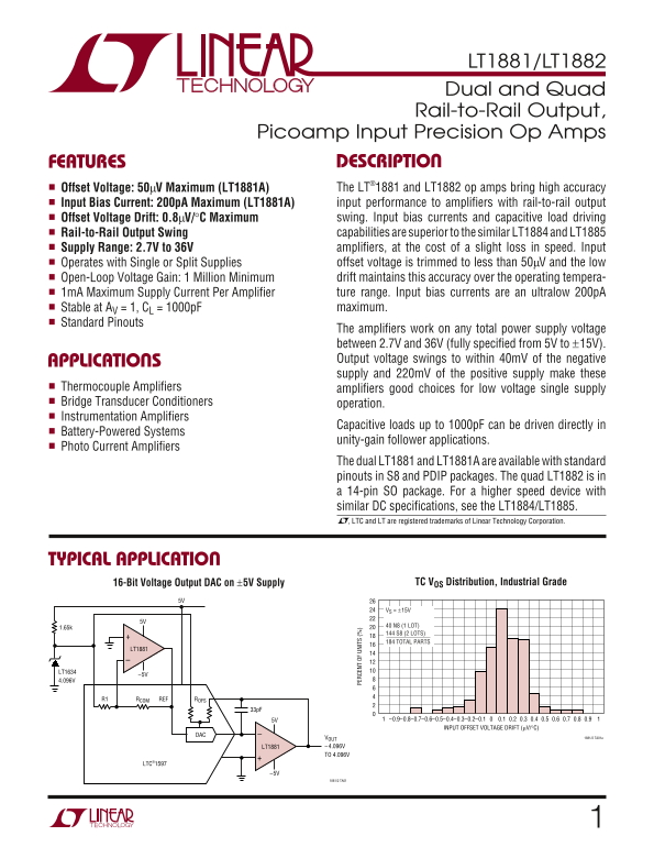
16-Bit Voltage Output DAC on ±5V Supply TC VOS Distribution, Industrial Grade

VS = ±15V

1.65k 40 N8 (1 LOT) 144 S8 (2 LOTS) 184 TOTAL PARTS

LT1881

LT1634

RCOM ROFSREFR1

INPUT OFFSET VOLTAGE DRIFT (µV/°C)

VOUT 1881/2 TA01a

LT1881 –4.096V TO 4.096V

LTC®1597

1881/2 TA01

Page Summary Contents For LINEAR TECHNOLOGY LT1881 LT1882 User's Manual

Page 1 LT1881/LT1882 Dual and Quad Rail-to-Rail Output, Picoamp Input Precision Op Amps FEATURES DESCRIPTIO Offset Voltage: 50µV Maximum (LT1881A) The LT®1881 and LT1882 op amps bring high accuracy Input Bia...
Page 2 LT1881/LT1882 ABSOLUTE AXI RATI GS (Note 1) Supply Voltage (V+ to V 40V Operating Temperature Range (Note 4) –40°C to 85°C Differential Input Voltage (Note 2) ±10V Specified Temperature Range (Note 5)...
Page 3 LT1881/LT1882 ELECTRICAL CHARACTERISTICS The ● denotes the specifications which apply over the full operating temperature range, otherwise specifications are at TA = 25°C. Single supply operation VS =...
Page 4 LT1881/LT1882 ELECTRICAL CHARACTERISTICS The ● denotes the specifications which apply over the full operating temperature range, otherwise specifications are at TA = 25°C. Single supply operation VS =...
Page 5 LT1881/LT1882 ELECTRICAL CHARACTERISTICS The ● denotes the specifications which apply over the full operating temperature range, otherwise specifications are at TA = 25°C. Split supply operation VS = ...
Page 6 LT1881/LT1882 ELECTRICAL CHARACTERISTICS The ● denotes the specifications which apply over the full operating temperature range, otherwise specifications are at TA = 25°C. Split supply operation VS = ...
Page 7 PH AS AR GI (D EG OU TP UT TE (V SU PP LY UR RE NT ER PL IF IE (µ A) LT1881/LT1882 TYPICAL PERFOR A CE CHARACTERISTICS Supply Current per Amplifier vs Supply Voltage Slew Rate vs Supply Voltage Slew R...
Page 8 UT (2 0m V/ DI V) UT (5 V/ DI V) LT1881/LT1882 GA IN (d B) TYPICAL PERFOR A CE CHARACTERISTICS Gain vs Frequency with CLOAD, Gain vs Frequency with CLOAD, AV = 1 AV = –1 VS = ±15V VS = ±15V (2 0m V/ D...
Page 9 IN PU CO ON OD VO LT AG (V (p A) IA PE RC EN OF NI TS LT1881/LT1882 TYPICAL PERFOR A CE CHARACTERISTICS LT1881 VOS Distribution, LT1881IS8 Voltage Offset vs TA = 25°C Temperature Warm-Up Drift vs Time...
Page 10 GA IN AN DW ID TH RO DU CT (K Hz LO OP AI (d B) OU TP UT AT UR AT IO VO LT AG (V LT1881/LT1882 TYPICAL PERFOR A CE CHARACTERISTICS LT1881 Output Saturation Voltage LT1881 Output Short-Circuit LT1881 O...
Page 11 SE RI ES UT PU RE SI ST AN CE (Ω NO IS CU RR EN DE NS IT (f A /√ Hz CM RR (d B) LT1881/LT1882 TYPICAL PERFOR A CE CHARACTERISTICS Common Mode Rejection Ratio vs LT1881 Noise Voltage vs Frequency LT188...
Page 12 LT1881/LT1882 GA IN (V /µ V) TH NO IS TYPICAL PERFOR A CE CHARACTERISTICS LT1881 Total Harmonic Distortion + Noise vs Output Voltage Amplitude LT1881 Open-Loop Gain f = 1k Hz AV = –1 RF = RG = 10k RL ...
Page 13 LT1881/LT1882 APPLICATIO S I FOR ATIO The LT1881 dual and LT1882 quad op amps feature PC board layout is important to insure that leakage cur- exceptional input precision with rail-to-rail output swin...
Page 14 LT1881/LT1882 PACKAGE DESCRIPTIO Dimensions in inches (millimeters) unless otherwise noted. N8 Package 8-Lead PDIP (Narrow 0.300) (LTC DWG # 05-08-1510) 0.400* (10.160) MAX 0.065 (1.651) 0.009 – 0.015...
Page 15 LT1881/LT1882 PACKAGE DESCRIPTIO Dimensions in inches (millimeters) unless otherwise noted. S8 Package 8-Lead Plastic Small Outline (Narrow 0.150) (LTC DWG # 05-08-1610) (0.203 – 0.254) 0°– 8° TYP (0....
Page 16 LT1881/LT1882 TYPICAL APPLICATIO –50°C to 600°C Digital Thermometer Operates on 3.3V VCC = 3.3V RF 1k VREF VCC CLK 1µF+IN RT R3 1/2 LT1881 LTC1287 1k –IN DOUT GND CS/SHDN 10k A1 0.1% 1/2 LT1881 VCC RT...

Manual Details

Brand Linear
Pages 16
File Size 256.25 KB
Published June 06, 2026
27 views

Enter the captcha to get the download link:

captcha

Frequently Asked Questions

What is the recommended voltage supply range for these op amps?

They can operate on any total power supply voltage between 2.7V and 36V.

How do I reduce offset voltage when using a single supply?

The devices are designed to handle single or split supplies, which helps keep the offset voltage at less than 50mV.

What loads can these amplifiers drive directly?

They can drive capacitive loads up to 1000pF in unity-gain follower applications.

What is the maximum input bias current for LT1882s?

The input bias current (LT1881/LT1882) is typically around 500 pA at room temperature.