# A B C D E F G H I J K L M N O P Q R S T U V W X Y Z

LINEAR TECHNOLOGY LT1715 User's Manual

Summary

Experience superior high-speed signal processing with the LT1715 UltraFast Dual Comparator. This component delivers exceptional performance up to 150MHz toggle frequency while maintaining an ultra-low power profile. The manual provides comprehensive technical specifications, application circuits for line receiving and level translation, and detailed guidelines for integrating this comparator into complex systems. Ideal for electrical engineers designing robust, low-power, high-speed logic interfaces requiring accurate signal detection across various voltage and differential input ranges (e.g., TTL/CMOS).
📄 Preview PAGE OF 16

Page 1 Text Content

LT1715 4ns, 150MHz

Dual Comparator with

Independent Input/Output Supplies

FEATURES DESCRIPTIO Ultra Fast: 4ns at 20m V Overdrive The LT®1715 is an Ultra Fast TM dual comparator optimized 150MHz Toggle Frequency for low voltage operation. Separate supplies allow inde- Separate Input and Output Power Supplies pendent analog input ranges and output logic levels with Low Power: 4.6m A per Comparator at 3V no loss of performance. The input voltage range extends Pinout Optimized for High Speed Use from 100m V below VEE to 1.2V below VCC. Internal hyster- Output Optimized for 3V and 5V Supplies esis makes the LT1715 easy to use even with slow moving TTL/CMOS Compatible Rail-to-Rail Output input signals. The rail-to-rail outputs directly interface to Input Voltage Range Extends 100m V TTL and CMOS. The symmetric output drive results in Below Negative Rail similar rise and fall times that can be harnessed for analog Internal Hysteresis with Specified Limits applications or for easy translation to other single supply

logic levels. APPLICATIO S The LT1715 is available in the 10-pin MSOP package. The pinout of the LT1715 minimizes parasitic effects by plac-

High Speed Differential Line Receivers

ing the most sensitive inputs away from the outputs,

Level Translators

shielded by the power rails.

Window Comparators

For a dual/quad single supply comparator with similar

Crystal Oscillator Circuits

propagation delay, see the LT1720/LT1721. For a single

Threshold Detectors/Discriminators

comparator with similar propagation delay, see the LT1719.

High Speed Sampling Circuits

, LTC and LT are registered trademarks of Linear Technology Corporation.

Delay Lines

Ultra Fast is a trademark of Linear Technology Corporation.

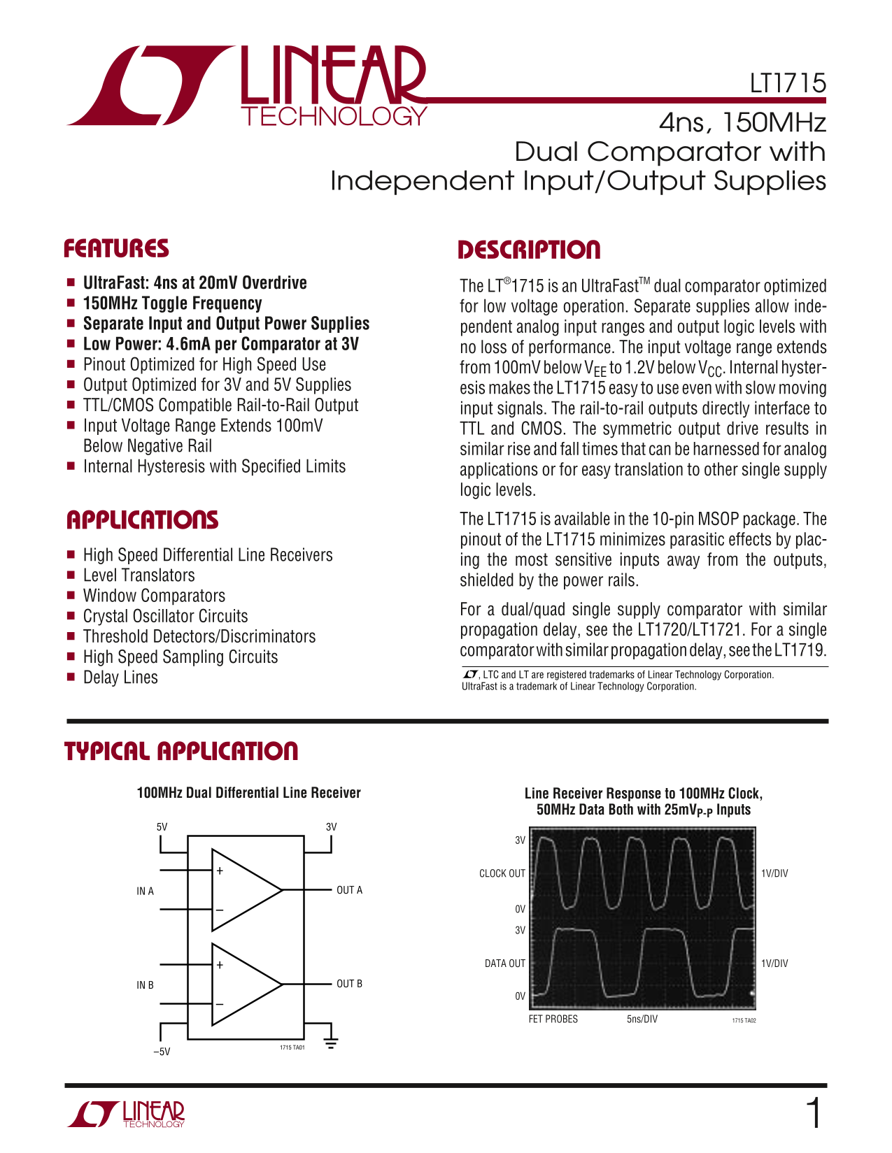
TYPICAL APPLICATIO 100MHz Dual Differential Line Receiver Line Receiver Response to 100MHz Clock,

50MHz Data Both with 25m VP-P Inputs

CLOCK OUT 1V/DIV

IN A OUT A

DATA OUT 1V/DIV

IN B OUT B

FET PROBES 5ns/DIV 1715 TA02

1715 TA01

Page Summary Contents For LINEAR TECHNOLOGY LT1715 User's Manual

Page 1 LT1715 4ns, 150MHz Dual Comparator with Independent Input/Output Supplies FEATURES DESCRIPTIO Ultra Fast: 4ns at 20m V Overdrive The LT®1715 is an Ultra Fast TM dual comparator optimized 150MHz Toggle...
Page 2 LT1715 ABSOLUTE AXI U RATI GS PACKAGE/ORDER I FOR ATIO (Note 1) Supply Voltage ORDER PART +VS to GND 7V NUMBER VCC to VEE 13.2V TOP VIEW LT1715CMS +VS to VEE 13.2V +IN A VCC –IN A +VS LT1715IMS VEE to...
Page 3 LT1715 ELECTRICAL CHARACTERISTICS The ● denotes specifications that apply over the full operating temperature range, otherwise specifications are at TA = 25°C. VCC = 5V, VEE = –5V, +VS = 5V, VCM = 1V,...
Page 4 OU TP UT OL TA GE (V IN PU BI AS (µ A) AN TR IP OI NT OL TA GE (m V) LT1715 TYPICAL PERFOR A CE CHARACTERISTICS Input Offset and Trip Voltages Input Offset and Trip Voltages Input Common Mode Limits v...
Page 5 TO GG LE RE QU EN CY (M Hz TO GG LE RE QU EN CY (M Hz PR OP AG AT IO DE LA (n s) LT1715 TYPICAL PERFOR A CE CHARACTERISTICS Propagation Delay Propagation Delay Propagation Delay vs Overdrive vs Temper...
Page 6 LT1715 PI FU CTIO S +IN A (Pin 1): Noninverting Input of Comparator A. GND (Pin 6): Ground for Output Stage. –IN A (Pin 2): Inverting Input of Comparator A. OUT B (Pin 7): Output of Comparator B. –IN ...
Page 7 LT1715 TEST CIRCUITS Response Time Test Circuit +Vs – VCM VCC – VCM DUT 10× SCOPE PROBE 25Ω 1/2 LT1715 50k (CIN ≈ 10p F) PULSE 2N3866 IN0V 1N5711 VEE – VCM *V1 = –1000 • (OVERDRIVE + VTRIP NOTE: RISIN...
Page 8 LT1715 APPLICATIO S I FOR ATIO responds correctly to a small differential input signal. If equal to the supply voltage, limited only by the absolute one input is within the common mode limit, the othe...
Page 9 LT1715 APPLICATIONS INFORMATION The ground pin of the LT1715 can disturb the ground plane maintain signal integrity. The LT1715 can drive DC termi- potential while toggling due to the extremely fast o...
Page 10 LT1715 APPLICATIO S I FOR ATIO At frequencies well beyond 100MHz, the toggling of one channel may be impaired by toggling on the other. This is VOH a rather complex interaction of supply bypassing and...
Page 11 LT1715 APPLICATIONS INFORMATION VREF R3 R1 may also be required. Note that the currents through the R1/R2 bias string should be many times the input currents of the LT1715. For 5% accuracy, the curren...
Page 12 LT1715 APPLICATIONS INFORMATION DO NOT USE FOR LT1715 LEVEL TRANSLATION. SEE TEXT LSTTL 270Ω 10KH/E (a) STANDARD TTL TO PECL TRANSLATOR +VS R1 R2 R3 1/2 LT1715 10KH/E 5V OR 5.2V 510Ω 180Ω 750Ω R3 100K...
Page 13 LT1715 APPLICATIO S I FOR ATIO The level translator designs assume one gate load. Mul- The input stage topology maximizes the input dynamic tiple gates can have significant IIH loading, and the trans-...
Page 14 LT1715 APPLICATIO S I FOR ATIO the frequency-dependent increase in power consumption. will easily leave this undesired operating mode no worse The frequency dependence of the supply current is shown f...
Page 15 LT1715 APPLICATIO S I FOR ATIO ±VTRIP Test Circuit Because the triangle wave is attenuated 1000:1 and fed to the LT1715’s differential input, the sampled voltages are The input trip points test circui...
Page 16 LT1715 TYPICAL APPLICATIO High Performance Sine Wave Similar delay performance is achieved with input frequen- to Square Wave Converter cies as high as 50MHz. There is, however, some additional encroa...

Manual Details

Brand Linear
Pages 16
File Size 242.35 KB
Published July 15, 2026
1 views

Enter the captcha to get the download link:

captcha

Frequently Asked Questions

What is the maximum toggle frequency of the LT1715?

The maximum toggle frequency is 150 MHz.

Does it support multiple supply voltages and input types?

Yes, it supports dual/quad single supplies and has TTL/CMOS compatible rail-to-rail outputs. It operates with a wide input voltage range of -1.2V to 1.2V.

How is the LT1715 packaged?

The device is available in the 10-pin MSOP package.

What is the operating temperature range?

Its specified operating temperature range is –40°C to 85°C.