LINEAR TECHNOLOGY LT1630 LT1631 Data Sheet Manual
Summary
Precision dual and quad operational amplifiers featuring a 30MHz bandwidth, 10V/ms slew rate, and true rail-to-rail performance. These low-power op amps deliver high signal integrity while maintaining excellent DC accuracy over wide supply ranges (2.7V to 36V). The manual provides comprehensive technical data covering electrical characteristics, packaging options, and typical applications—making it ideal for engineers designing active filters, buffers, or advanced signal processing systems requiring maximum reliability and performance in demanding environments.
Page 1 Text Content
LT1630/LT1631
30MHz, 10V/µs, Dual/Quad Rail-to-Rail Input and Output Precision Op Amps
FEATURES DESCRIPTION Gain-Bandwidth Product: 30MHz The LT®1630/LT1631 are dual/quad, rail-to-rail input and Slew Rate: 10V/µs output op amps with a 30MHz gain-bandwidth product and Low Supply Current per Amplifier: 3.5m A a 10V/µs slew rate. Input Common Mode Range Includes Both Rails
The LT1630/LT1631 have excellent DC precision over the
Output Swings Rail-to-Rail
full range of operation. Input offset voltage is typically less
Input Offset Voltage, Rail-to-Rail: 525µV Max
than 150µV and the minimum open-loop gain of one
Input Offset Current: 150n A Max
million into a 10k load virtually eliminates all gain error. To
Input Bias Current: 1000n A Max
maximize common mode rejection, the LT1630/LT1631
Open-Loop Gain: 1000V/m V Min
employ a patented trim technique for both input stages,
Low Input Noise Voltage: 6n V/√Hz Typ
one at the negative supply and the other at the positive
Low Distortion: – 91d Bc at 100k Hz
supply, that gives a typical CMRR of 106d B over the full
Wide Supply Range: 2.7V to ±15V
input range.
Large Output Drive Current: 35m A Min
Dual in 8-Pin PDIP and SO Packages The LT1630/LT1631 maintain their performance for sup- Quad in Narrow 14-Pin SO Package plies from 2.7V to 36V and are specified at 3V, 5V and ±15V GA IN (d B) supplies. The inputs can be driven beyond the supplies without damage or phase reversal of the output. The
APPLICATIONS
output delivers load currents in excess of 35m A.
Active Filters
The LT1630 is available in 8-pin PDIP and SO packages
Rail-to-Rail Buffer Amplifiers
with the standard dual op amp pinout. The LT1631 features
Driving A/D Converters
the standard quad op amp configuration and is available in
Low Voltage Signal Processing
a 14-pin plastic SO package. These devices can be used as
Battery-Powered Systems
plug-in replacements for many standard op amps to
, LTC and LT are registered trademarks of Linear Technology Corporation. improve input/output range and performance.
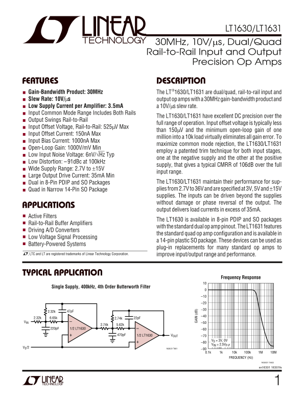
TYPICAL APPLICATION
Frequency Response
Single Supply, 400k Hz, 4th Order Butterworth Filter
2.32k 6.65k 2.74k 22p F VIN –50
220p F 1/2 LT1630 –60
470p F 1/2 LT1630 VOUT
–70 VS = 3V, 0V –80 VIN = 2.5VP-P
VS/2 1630/31 TA01
0.1k 1k 10k 100k 1M 10M FREQUENCY (Hz)
1630/31 TA02
sn16301 16301fs
Page Summary Contents For LINEAR TECHNOLOGY LT1630 LT1631 Data Sheet Manual
Manual Details
| Brand | Linear |
|---|---|
| Pages | 16 |
| File Size | 282.90 KB |
| Published | June 16, 2026 |
Enter the captcha to get the download link:

Frequently Asked Questions
What is the typical input noise voltage of the LT1630/LT1631?
The low input noise voltage is typically 6nV/√Hz at 1kHz.
Can this op amp operate rail-to-rail with a single power supply?
Yes, the output swings cover the full rail-to-rail range of operation.
What are the maximum recommended operating temperatures?
The specified temperature range is -40°C to 85°C for general operation.
How large is the open-loop gain and slew rate?
It has a minimum open-loop gain of 1000V/mV and a maximum slew rate of 10V/ms.