# A B C D E F G H I J K L M N O P Q R S T U V W X Y Z

LINEAR TECHNOLOGY LT1366 LT1367 LT1368 LT1369 User Manual and Technical Specifications

Summary

These high-precision dual and quad rail-to-rail operational amplifiers are designed for demanding low voltage signal processing applications. Featuring wide supply ranges, low input offset voltage, and exceptional common mode rejection ratio, these op amps deliver stable performance even when driving A/D converters or requiring full output swings. The manual provides comprehensive coverage of electrical specifications, package options (PDIP, SO), and detailed application notes to ensure optimal integration into complex electronic circuits. Ideal for engineers seeking reliable, high-performance amplification across varying supply conditions.
📄 Preview PAGE OF 20

Page 1 Text Content

LT1366/LT1367 LT1368/LT1369

Dual and Quad Precision Rail-to-Rail Input and Output

Op Amps

FEATURES DESCRIPTION

Input Common Mode Range Includes Both Rails The LT®1366/LT1367/LT1368/LT1369 are dual and quad Output Swings Rail-to-Rail bipolar op amps which combine rail-to-rail input and Low Input Offset Voltage: 150µV output operation with precision specifications. These op High Common Mode Rejection Ratio: 90d B amps maintain their characteristics over a supply range of

High AVOL: >1V/µV Driving 10kΩ Load 1.8V to 36V. Operation is specified for 3V, 5V and ±15V Low Input Bias Current: 10n A supplies. Input offset voltage is typically 150µV, with an Wide Supply Range: 1.8V to ±15V open-loop gain AVOL of 1 million while driving a 10k load.

Low Supply Current: 375µA per Amplifier Common mode rejection is typically 90d B over the full rail- High Output Drive: 30m A to-rail input range, and supply rejection is 110d B. 400k Hz Gain-Bandwidth Product

The LT1366/LT1367 have conventional compensation

Slew Rate: 0.13V/µs

which assures stability for capacitive loads of 1000p F or

Stable for Capacitive Loads up to 1000p F

less. The LT1368/LT1369 have compensation that SA TU RA TI ON OL TA GE (m V) requires a 0.1µF output capacitor, which improves the

V OU

APPLICATIONS amplifier’s supply rejection and reduces output imped- ance at high frequencies. The output capacitor’s filtering

Rail-to-Rail Buffer Amplifiers

action reduces high frequency noise, which is beneficial

Low Voltage Signal Processing

when driving A/D converters.

Supply Current Sensing at Either Rail

The LT1366/LT1368 are available in plastic 8-pin PDIP and

Driving A/D Converters

8-lead SO packages with the standard dual op amp pinout. The LT1367/LT1369 feature the standard quad pinout, which is available in a plastic 14-lead SO package. These devices can be used as plug-in replacements for many standard op amps to improve input/output range and

, LTC and LT are registered trademarks of Linear Technology Corporation. precision.

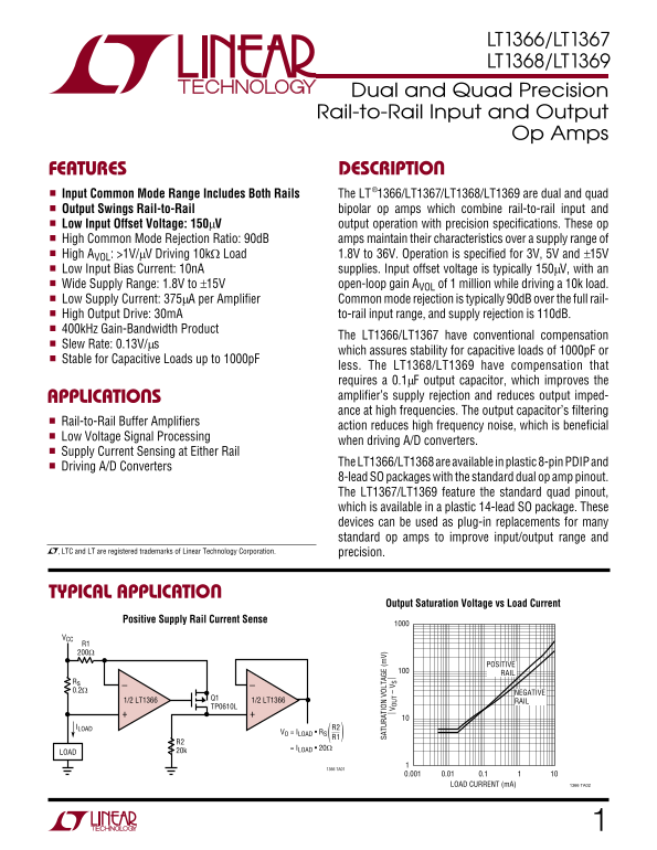
TYPICAL APPLICATION

Output Saturation Voltage vs Load Current

Positive Supply Rail Current Sense

VCC R1 200Ω

POSITIVE RAIL

Rs 0.2Ω

NEGATIVE

1/2 LT1366 1/2 LT1366 RAIL

TP0610L

ILOAD R2

VO = ILOAD • RS

= ILOAD • 20Ω

LOAD 20k

1366 TA01

LOAD CURRENT (m A) 1366 TA02

Page Summary Contents For LINEAR TECHNOLOGY LT1366 LT1367 LT1368 LT1369 User Manual and Technical Specifications

Page 1 LT1366/LT1367 LT1368/LT1369 Dual and Quad Precision Rail-to-Rail Input and Output Op Amps FEATURES DESCRIPTION Input Common Mode Range Includes Both Rails The LT®1366/LT1367/LT1368/LT1369 are dual and...
Page 2 LT1366/LT1367 LT1368/LT1369 ABSOLUTE MAXIMUM RATINGS + to V –) Total Supply Voltage (V 36V Junction Temperature.......................................... 150°C Input Current ±15m A Storage Temperature...
Page 3 LT1366/LT1367 LT1368/LT1369 ELECTRICAL CHARACTERISTICS TA = 25°C, VS = 5V, 0V, VCM = 2.5V, VO = 2.5V, unless otherwise noted. SYMBOL PARAMETER CONDITIONS MIN TYP MAX UNITS IOS Input Offset Current VCM...
Page 4 LT1366/LT1367 LT1368/LT1369 ELECTRICAL CHARACTERISTICS 0°C < TA < 70°C, VS = 5V, 0V, VCM = 2.5V, VO = 2.5V, unless otherwise noted. SYMBOL PARAMETER CONDITIONS MIN TYP MAX UNITS AVOL Large-Signa...
Page 5 LT1366/LT1367 LT1368/LT1369 ELECTRICAL CHARACTERISTICS 0°C < TA < 70°C, VS = 3V, 0V, VCM = 1.5V, VO = 1.5V, unless otherwise noted. SYMBOL PARAMETER CONDITIONS MIN TYP MAX UNITS VOS Input Offset...
Page 6 LT1366/LT1367 LT1368/LT1369 ELECTRICAL CHARACTERISTICS TA = 25°C, VS = ±15V, VCM = 0V, VO = 0V, unless otherwise noted. SYMBOL PARAMETER CONDITIONS MIN TYP MAX UNITS VOS Input Offset Voltage (LT1366/L...
Page 7 LT1366/LT1367 LT1368/LT1369 ELECTRICAL CHARACTERISTICS 0°C < TA < 70°C, VS = ±15V, VCM = 0V, VO = 0V, unless otherwise noted. SYMBOL PARAMETER CONDITIONS MIN TYP MAX UNITS VOS Input Offset Volta...
Page 8 LT1366/LT1367 IN PU BI AS UR RE NT (n A) SU PP LY UR RE NT ER PL IF IE (µ A) PE RC EN OF NI TS LT1368/LT1369 TYPICAL PERFORMANCE CHARACTERISTICS (The data presented here applies to the LT1366/LT1367/L...
Page 9 LT1366/LT1367 CU RR EN NO IS (p A/ √H z) CO ON -M OD RE JE CT IO RA TI (d B) CH AN GE IN FF SE VO LT AG (µ V) PHASE SHIFT (DEG) LT1368/LT1369 TYPICAL PERFORMANCE CHARACTERISTICS (The data presented he...
Page 10 LT1366/LT1367 SL EW AT (V /µ s) OV ER SH OO FR EQ UE NC (k Hz LT1368/LT1369 TYPICAL PERFORMANCE CHARACTERISTICS (The data presented here applies to the LT1366/LT1367/LT1368/LT1369 unless otherwise not...
Page 11 LT1366/LT1367 TH NO IS LT1368/LT1369 TYPICAL PERFORMANCE CHARACTERISTICS (The data presented here applies to the LT1366/LT1367/LT1368/LT1369 unless otherwise noted.) Large-Signal Response Small-Signal...
Page 12 LT1366/LT1367 LT1368/LT1369 APPLICATIONS INFORMATION cated on Linear Technology’s proprietary complementary When overdriven, the amplifier draws input current that bipolar process, which ensures very ...
Page 13 LT1366/LT1367 0m V/ DI LT1368/LT1369 0m V/ DI APPLICATIONS INFORMATION Improved Supply Rejection in the LT1368/LT1369 Figure 4 shows the outputs of the LT1366/LT1368 per- turbed by a 200m VP-P 50k Hz ...
Page 14 LT1366/LT1367 LT1368/LT1369 TYPICAL APPLICATIONS Precision Low Dropout Regulator creases the regulator’s phase margin. Although not di- rectly part of the compensation, R9 decouples the op Microproces...
Page 15 LT1366/LT1367 LT1368/LT1369 TYPICAL APPLICATIONS High-Side Current Source input voltage, circuit operation is limited by the LT1366’s absolute maximum ratings and the output power require- The wide-co...
Page 16 LT1366/LT1367 LT1368/LT1369 GA IN (d B) TYPICAL APPLICATIONS the 2 op amp loop to create a negative summing junction at A1’s positive input1. The circuit has low sensitivities for V+ center frequency ...
Page 17 LT1366/LT1367 LT1368/LT1369 PACKAGE DESCRIPTION Dimensions in inches (millimeters) unless otherwise noted. N8 Package 8-Lead PDIP (Narrow 0.300) (LTC DWG # 05-08-1510) 0.400* (10.160) MAX 0.065 (1.651...
Page 18 LT1366/LT1367 LT1368/LT1369 PACKAGE DESCRIPTION Dimensions in inches (millimeters) unless otherwise noted. S8 Package 8-Lead Plastic Small Outline (Narrow 0.150) (LTC DWG # 05-08-1610) (0.203 – 0.254)...
Page 19 LT1366/LT1367 LT1368/LT1369 PACKAGE DESCRIPTION Dimensions in inches (millimeters) unless otherwise noted. S Package 14-Lead Plastic Small Outline (Narrow 0.150) (LTC DWG # 05-08-1610) 0° – 8° TYP DIM...
Page 20 LT1366/LT1367 LT1368/LT1369 TYPICAL APPLICATION Instrumentation Amplifier 1/4 10k 100k LT1367 GUARD RF 102k RG 11.3k INPUTS LT1367 LT1367 OUTPUT RG 11.3k GUARD RF 102k 1/4 10k 100k GAIN = 10 1 + = 100...

Manual Details

Brand Linear
Pages 20
File Size 341.30 KB
Published June 05, 2026
52 views

Enter the captcha to get the download link:

captcha

Frequently Asked Questions

What is the operating temperature range for these op amps?

The continuous operating temperature range is specified as –40°C to 85°C.

How do I connect the power supply when using the LT1368/LT1369?

These devices use compensation requiring a 0.1μF output capacitor, which enhances the amplifier's supply rejection and reduces output impedance.

What are the available package types for different models?

The LT1366/LT1368 come in 8-pin PDIP or 8-lead SO packages, while the LT1367/LT1369 use a standard quad pinout in a 14-lead SO package.