# A B C D E F G H I J K L M N O P Q R S T U V W X Y Z

LINEAR TECHNOLOGY LT1308A LT1308B User Manual and Technical Specifications

Summary

These micropower DC/DC boost converters are engineered to deliver stable 5V power from single or multiple Li-Ion cells at higher currents (up to 1A). The comprehensive manual details advanced features, including automatic burst mode operation for ultra-low quiescent current draw and enhanced low-battery detection accuracy. Designed for engineers developing portable electronics—such as GSM phones, digital cameras, and GPS receivers—it offers a high-efficiency solution suitable for battery backup and demanding outdoor applications requiring reliability across wide voltage ranges.
📄 Preview PAGE OF 20

Page 1 Text Content

LT1308A/LT1308B

High Current, Micropower Single Cell, 600k Hz DC/DC Converters FEATURES DESCRIPTIO 5V at 1A from a Single Li-Ion Cell The LT®1308A/LT1308B are micropower, fixed frequency 5V at 800m A in SEPIC Mode from Four Ni Cd Cells step-up DC/DC converters that operate over a 1V to 10V Fixed Frequency Operation: 600k Hz input voltage range. They are improved versions of the Boost Converter Outputs up to 34V LT1308 and are recommended for use in new designs. The Starts into Heavy Loads LT1308A features automatic shifting to power saving Automatic Burst Mode TM Operation at Burst Mode operation at light loads and consumes just Light Load (LT1308A) 140μA at no load. The LT1308B features continuous Continuous Switching at Light Loads (LT1308B) switching at light loads and operates at a quiescent current Low VCESAT Switch: 300m V at 2A of 2.5m A. Both devices consume less than 1μA in Pin-for-Pin Upgrade Compatible with LT1308 shutdown.

Lower Quiescent Current in Shutdown: 1μA (Max)

Low-battery detector accuracy is significantly tighter than

Improved Accuracy Low-Battery Detector

the LT1308. The 200m V reference is specified at ±2% at

Reference: 200m V ±2% EF FI CI EN CY

room and ±3% over temperature. The shutdown pin

Available in 8-Lead SO and 14-Lead TSSOP Packages

enables the device when it is tied to a 1V or higher source and does not need to be tied to VIN as on the LT1308. An APPLICATIO internal VC clamp results in improved transient response and the switch voltage rating has been increased to 36V,

GSM/CDMA Phones

enabling higher output voltage applications.

Digital Cameras

The LT1308A/LT1308B are available in the 8-lead SO and

LCD Bias Supplies

the 14-lead TSSOP packages.

Answer-Back Pagers GPS Receivers , LT, LTC and LTM are registered trademarks of Linear Technology Corporation. Burst

Mode is a registered trademark of Linear Technology Corporation. All other trademarks are

Battery Backup Supplies

the property of their respective owners.

Handheld Computers

TYPICAL APPLICATIO

Converter Efficiency

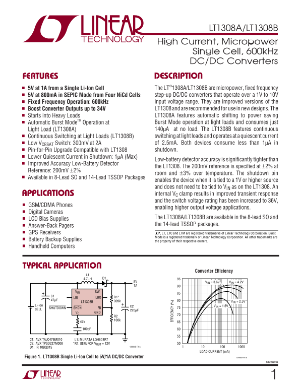
5V VIN = 3.6V VIN = 4.2V 1A

VIN SW

LBOLBI R1*

LT1308B 309k VIN = 2.5V

Li-Ion VIN = 1.5V

SHDNSHUTDOWN FB

VC GND

C1: AVX TAJC476M010 L1: MURATA LQH6C4R7 C2: AVX TPSD227M006 *R1: 887k FOR VOUT = 12V

D1: IR 10BQ015

LOAD CURRENT (m A)

Figure 1. LT1308B Single Li-Ion Cell to 5V/1A DC/DC Converter 1308A/B F01b

1308abfa

Page Summary Contents For LINEAR TECHNOLOGY LT1308A LT1308B User Manual and Technical Specifications

Page 1 LT1308A/LT1308B High Current, Micropower Single Cell, 600k Hz DC/DC Converters FEATURES DESCRIPTIO 5V at 1A from a Single Li-Ion Cell The LT®1308A/LT1308B are micropower, fixed frequency 5V at 800m A ...
Page 2 LT1308A/LT1308B XI ARBSOLUTE TI (Note 1) VIN, SHDN, LBO Voltage 10V Operating Temperature Range SW Voltage –0.4V to 36V Commercial 0°C to 70°C FB Voltage VIN + 1V Extended Commerial (Note 2) –40°C to ...
Page 3 LT1308A/LT1308B ELECTRICAL CHARACTERISTICS The ● denotes specifications which apply over the full operating temperature range, otherwise specifications are TA = 25°C. Commercial Grade 0°C to 70°C. VIN...
Page 4 EF FI CI EN CY LT1308A/LT1308B ELECTRICAL CHARACTERISTICS The ● denotes specifications which apply over the full operating temperature range, otherwise specifications are TA = 25°C. Industrial Grade –...
Page 5 FR EQ UE NC (k Hz SH DN IN UR RE NT (μ A) EF FI CI EN CY LT1308A/LT1308B TYPICAL PERFORMANCE CHARACTERISTICS LT1308B Switch Current Limit vs Switch Saturation Voltage 12V Output Efficiency Duty Cycle ...
Page 6 LT1308A/LT1308B PIN FUNCTIONS (SO/TSSOP) VC (Pin 1/Pin 1): Compensation Pin for Error Amplifier. SW (Pin 5/Pins 8, 9, 10): Switch Pins. Connect inductor/ Connect a series RC from this pin to ground. T...
Page 7 LT1308A/LT1308B BLOCK DIAGRA S Q4 2VBE SHUTDOWN ERROR LBO (EXTERNAL) FB AMPLIFIER ENABLE ×10 BIAS (EXTERNAL) 30k SW COMPARATOR DRIVER R4 FF 140k GENERATOR Q3Q 600k Hz OSCILLATOR *HYSTERESIS IN LT1308A...
Page 8 LT1308A/LT1308B APPLICATIONS INFORMATION OPERATION Low-battery detector A4’s open-collector output (LBO) pulls low when the LBI pin voltage drops below 200m V. The LT1308A combines a current mode, fix...
Page 9 LT1308A/LT1308B APPLICATIONS INFORMATION Waveforms for a LT1308B 5V to 12V boost converter LAYOUT HINTS using a 10μF ceramic output capacitor are pictured in The LT1308A/LT1308B switch current at high...
Page 10 LT1308A/LT1308B APPLICATIONS INFORMATION A SEPIC (Single-Ended Primary Inductance Converter) LBOLBI GROUND PLANE schematic is shown in Figure 8. This converter topology C1 produces a regulated output ...
Page 11 LT1308A/LT1308B APPLICATIONS INFORMATION SHDN PIN A cross plot of the low-battery detector is shown in Figure 12. The LBI pin is swept with an input which varies The LT1308A/LT1308B SHDN pin is improv...
Page 12 LT1308A/LT1308B APPLICATIONS INFORMATION when operating from a battery composed of alkaline cells. The inrush current may cause sufficiency internal 1V/DIV voltage drop to trigger a low-battery indica...
Page 13 LT1308A/LT1308B APPLICATIONS INFORMATION 12V so that copper loss is minimized. Acceptable inductance values range between 2μH and 20μH, with 4.7μH best for 5V/DIV 5V most applications. Lower value ind...
Page 14 LT1308A/LT1308B APPLICATIONS INFORMATION Ceramic Capacitors Without CPL, load step response is pictured in Figure 22. Although the output settles faster than the tantalum case, Multilayer ceramic capa...
Page 15 LT1308A/LT1308B APPLICATIONS INFORMATION VOUT VOUT 500m V/DIV VIN = 4.2V VOUT VIN = 3.6V IL1 1A/DIV VOUT VIN = 3V 500m A ILOAD CURRENT 200μs/DIV VOUT TRACES = 200μs/DIV 1308 F23 200m V/DIV 1308 F25 Fi...
Page 16 LT1308A/LT1308B TYPICAL APPLICATIO S Triple Output TFTLCD Bias Supply VOFF –9V D3 VON VIN 5V AVDD 10V VIN SW 500m A SHDN 76.8k C1 LT1308B VC FB 220k GND C1:TAIYO-YUDEN JMK212BJ475MG 1308 TA02 C2, C3:T...
Page 17 LT1308A/LT1308B TYPICAL APPLICATIO S 40n F EL Panel Driver VBAT 1:12 3V TO 6V 3.3V REGULATED VIN SW Q1 FBLBO 2M LT1308A 17k 150k 324k C2 LBI SHDN SHUTDOWN 1μF 200V GNDVC Q2 400V EL PANEL 1308 TA03 C1:...
Page 18 LT1308A/LT1308B PACKAGE DESCRIPTION S8 Package 8-Lead Plastic Small Outline (Narrow .150 Inch) (Reference LTC DWG # 05-08-1610) NOTE 3 .050 BSC MIN .150 – .157 NOTE 3 .030 ±.005 TYP RECOMMENDED SOLDER...
Page 19 LT1308A/LT1308B PACKAGE DESCRIPTION F Package 14-Lead Plastic TSSOP (4.4mm) (Reference LTC DWG # 05-08-1650) (.252) BSC 0.05 0.65 BSC0.45 ± RECOMMENDED SOLDER PAD LAYOUT 0.25 MAX REF 0° – 8° 0.65 0.09...
Page 20 LT1308A/LT1308B TYPICAL APPLICATIO Li-Ion to 12V/300m A Step-Up DC/DC Converter 2.7V TO 4.2V VIN SW LT1308B 887k Li-Ion SHDNSHUTDOWN FB VC GND C1: AVX TAJC476M010 L1: MURATA LQH6C4R7 C2: AVX TPSD107M0...

Manual Details

Brand Linear
Pages 20
File Size 777.17 KB
Published June 16, 2026
6 views

Enter the captcha to get the download link:

captcha

Frequently Asked Questions

What is the operating voltage range for the LT1308A/LT1308B?

The device operates over a 1V to 10V input range, and the switch voltage rating has been increased to 36V.

How do these converters perform under light load conditions?

The LT1308A uses Automatic Burst Mode operation for light loads (140μA at no load), while the LT1308B features continuous switching and operates at 2.5mA quiescent current.

Are there design compatibility considerations with older models?

Yes, they are pin-for-pin upgrade compatible with the LT1308 shutdown and feature a lower quiescent shutdown current of 1μA (Max).

What temperature ranges are available for these components?

They are available in commercial operational temperatures (0°C to 70°C) or industrial extended range (-40°C to 85°C).