LINEAR LTC4311 User Guide and Technical Specifications
Summary
Optimize signal integrity for I²C and SMBus communications with this advanced Bus Accelerator. It solves critical limitations of open-drain buses by supplying strong, slew rate-controlled pull-up current across wide voltage ranges (1.6V–5.5V). Ideal for complex systems like notebooks, storage arrays, or servers featuring numerous hot-swappable I/O cards and high bus capacitance. The manual details its operation, proving reliable communication even under extreme varying loads.
Page 1 Text Content
L DESIGN FEATURES
Increase I2C or SMBus Data Rate and Reduce Power Consumption with
Low Power Bus Accelerator by Sam Tran
Introduction
VCC VCC
I2C and SMBus 2‑wire buses use 1.6V LTC4311 1.6V
simple open‑drain pull‑down drivers VCC BUS1
with resistive or current source pull‑ ENABLE
ups. Communications protocols in GND BUS2 these systems allow multiple devices
I2C to drive and monitor the bus without SCL SDA
bus contention, creating a robust communications link. Unfortunately,
CLK DATA CLK DATA as systems trend towards higher com‑ IN IN IN IN
plexity and lower supply voltages, the
CLK DATA CLK DATA advantages gained by the simplicity OUT OUT OUT OUT
of the open‑drain pull‑down protocol
DEVICE 1 DEVICE N
are offset by the disadvantages of increased rise times and greater DC
Figure 1. Typical LTC4311 low voltage application circuit
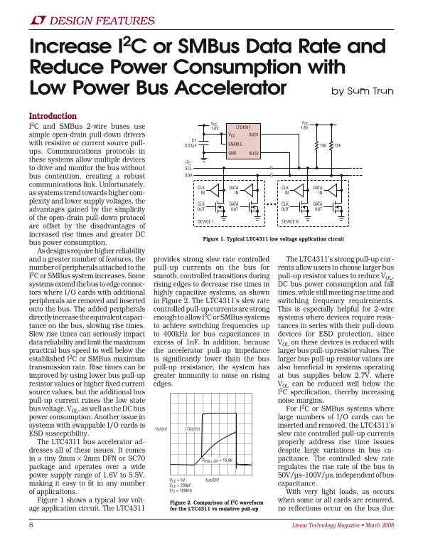
bus power consumption. As designs require higher reliability and a greater number of features, the provides strong slew rate controlled The LTC4311’s strong pull‑up cur‑ number of peripherals attached to the pull‑up currents on the bus for rents allow users to choose larger bus I2C or SMBus system increases. Some smooth, controlled transitions during pull‑up resistor values to reduce VOL, systems extend the bus to edge connec‑ rising edges to decrease rise times in DC bus power consumption and fall tors where I/O cards with additional highly capacitive systems, as shown times, while still meeting rise time and peripherals are removed and inserted in Figure 2. The LTC4311’s slew rate switching frequency requirements. onto the bus. The added peripherals controlled pull‑up currents are strong This is especially helpful for 2‑wire directly increase the equivalent capaci‑ enough to allow I2C or SMBus systems systems where devices require resis‑ tance on the bus, slowing rise times. to achieve switching frequencies up tances in series with their pull‑down Slow rise times can seriously impact to 400k Hz for bus capacitances in devices for ESD protection, since data reliability and limit the maximum excess of 1n F. In addition, because VOL on these devices is reduced with practical bus speed to well below the the accelerator pull‑up impedance larger bus pull‑up resistor values. The established I2C or SMBus maximum is significantly lower than the bus larger bus pull‑up resistor values are transmission rate. Rise times can be pull‑up resistance, the system has also beneficial in systems operating
improved by using lower bus pull‑up greater immunity to noise on rising at bus supplies below 2.7V, where
resistor values or higher fixed current edges. VOL can be reduced well below the source values, but the additional bus I2C specification, thereby increasing pull‑up current raises the low state noise margins. bus voltage, VOL, as well as the DC bus For I2C or SMBus systems where power consumption. Another issue in large numbers of I/O cards can be systems with swappable I/O cards is inserted and removed, the LTC4311’s
LTC43111V/DIV
ESD susceptibility. slew rate controlled pull‑up currents The LTC4311 bus accelerator ad‑ properly address rise time issues dresses all of these issues. It comes despite large variations in bus ca‑ in a tiny 2mm × 2mm DFN or SC70 RPULL-UP = 15.8k pacitance. The controlled slew rate package and operates over a wide regulates the rise rate of the bus to power supply range of 1.6V to 5.5V, 50V/µs–100V/µs, independent of bus
VCC = 5V 1µs/DIV
making it easy to fit in any number CLD = 200p F capacitance.
f I2C = 100k Hz
of applications. With very light loads, as occurs Figure 1 shows a typical low volt‑ when some or all cards are removed,
Figure 2. Comparison of I2C waveform
age application circuit. The LTC4311 for the LTC4311 vs resistive pull-up no reflections occur on the bus due
Linear Technology Magazine • March 2008
Page Summary Contents For LINEAR LTC4311 User Guide and Technical Specifications
Manual Details
| Brand | Linear |
|---|---|
| Pages | 3 |
| File Size | 214.87 KB |
| Published | June 16, 2026 |
Enter the captcha to get the download link:
