# A B C D E F G H I J K L M N O P Q R S T U V W X Y Z

LINEAR TECHNOLOGY LTC3722-1 User Guide and Specifications Book LTC3722-2 User Manual and Technical Documentation

Summary

Optimize your power delivery systems with this dual-mode full bridge controller, engineered for high efficiency Zero Voltage Switching (ZVS) converters. Featuring adaptive ZVS circuits and configurable protection options, it ensures optimal performance in critical infrastructure applications. The detailed manual provides technical deep-dive on advanced features like programmable delay control, comprehensive UVLO management, and low quiescent current operation. Essential for engineers designing reliable power solutions for telecom, data centers, and distributed power architectures.
📄 Preview PAGE OF 28

Page 1 Text Content

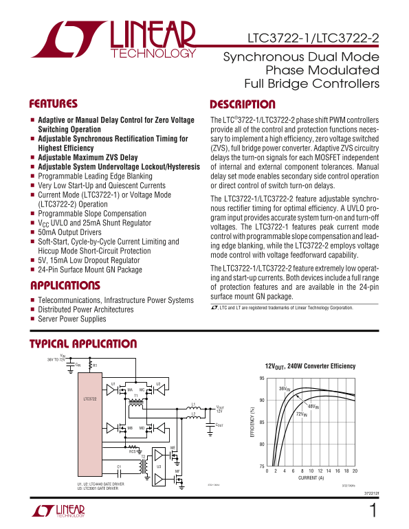
LTC3722-1/LTC3722-2 Synchronous Dual Mode Phase Modulated Full Bridge Controllers

FEATURES DESCRIPTIO Adaptive or Manual Delay Control for Zero Voltage The LTC®3722-1/LTC3722-2 phase shift PWM controllers Switching Operation provide all of the control and protection functions neces- Adjustable Synchronous Rectification Timing for sary to implement a high efficiency, zero voltage switched Highest Efficiency (ZVS), full bridge power converter. Adaptive ZVS circuitry Adjustable Maximum ZVS Delay delays the turn-on signals for each MOSFET independent

Adjustable System Undervoltage Lockout/Hysteresis of internal and external component tolerances. Manual Programmable Leading Edge Blanking delay set mode enables secondary side control operation Very Low Start-Up and Quiescent Currents or direct control of switch turn-on delays.

Current Mode (LTC3722-1) or Voltage Mode

The LTC3722-1/LTC3722-2 feature adjustable synchro-

(LTC3722-2) Operation

nous rectifier timing for optimal efficiency. A UVLO pro-

Programmable Slope Compensation

gram input provides accurate system turn-on and turn-off

VCC UVLO and 25m A Shunt Regulator

voltages. The LTC3722-1 features peak current mode

50m A Output Drivers

control with programmable slope compensation and lead-

Soft-Start, Cycle-by-Cycle Current Limiting and

ing edge blanking, while the LTC3722-2 employs voltage

Hiccup Mode Short-Circuit Protection EF FI CI EN CY

mode control with voltage feedforward capability.

5V, 15m A Low Dropout Regulator

24-Pin Surface Mount GN Package The LTC3722-1/LTC3722-2 feature extremely low operat- ing and start-up currents. Both devices include a full range

APPLICATIO S of protection features and are available in the 24-pin

surface mount GN package.

Telecommunications, Infrastructure Power Systems

, LTC and LT are registered trademarks of Linear Technology Corporation.

Distributed Power Architectures Server Power Supplies

TYPICAL APPLICATIO VIN 36V TO 72V

CIN R1

12VOUT, 240W Converter Efficiency

MA MC 36VIN

LTC3722

VOUT 48VIN

L2 72VIN

MB MD

RCS T2

CURRENT (A)

3722 • TA01AU1, U2: LTC4440 GATE DRIVER 3722 TA01b

U3: LTC3901 GATE DRIVER

Page Summary Contents For LINEAR TECHNOLOGY LTC3722-1 User Guide and Specifications Book LTC3722-2 User Manual and Technical Documentation

Page 1 LTC3722-1/LTC3722-2 Synchronous Dual Mode Phase Modulated Full Bridge Controllers FEATURES DESCRIPTIO Adaptive or Manual Delay Control for Zero Voltage The LTC®3722-1/LTC3722-2 phase shift PWM control...
Page 2 LTC3722-1/LTC3722-2 ABSOLUTE AXI RATI GS (Note 1) VCC to GND (Low Impedance Source) –0.3 to 10V VREF Output Current Self Regulated (Chip Self Regulates at 10.3V) Outputs (A,B,C,D,E,F) Current ±100m A ...
Page 3 LTC3722-1/LTC3722-2 ELECTRICAL CHARACTERISTICS The ● denotes the specifications which apply over the full operating temperature range, otherwise specifications are at TA = 25°C. VCC = 9.5V, CT = 270p ...
Page 4 LTC3722-1/LTC3722-2 ELECTRICAL CHARACTERISTICS The ● denotes the specifications which apply over the full operating temperature range, otherwise specifications are at TA = 25°C. VCC = 9.5V, unless oth...
Page 5 PH AS (D EG GA IN (d B) BL AN TI (n s) (µ A) LTC3722-1/LTC3722-2 TYPICAL PERFOR A CE CHARACTERISTICS Oscillator Frequency vs Start-Up ICC vs VCC VCC vs ISHUNT Temperature TA = 25°C TA = 25°C CT = 270p...
Page 6 FB OL TA GE (V CU RR EN (µ A) LTC3722-1/LTC3722-2 TYPICAL PERFOR A CE CHARACTERISTICS DE LA (n S) VCC Shunt Voltage vs Delay Pin Threshold vs Slope Current vs Temperature Temperature Temperature 10.5 ...
Page 7 LTC3722-1/LTC3722-2 PI FU CTIO S (LTC3722-1/LTC3722-2) SYNC (Pin 1/Pin 1): Synchronization Input/Output for the SBUS (Pin 10/Pin 10): Line Voltage Sense Input. SBUS is Oscillator. The input threshold ...
Page 8 LTC3722-1/LTC3722-2 PI FU CTIO S (LTC3722-1/LTC3722-2) OUTC (Pin 19/Pin 19): 50m A Driver for High Side of the PGND. Connect the ceramic VCC bypass capacitor directly Full Bridge Active Leg. to PGND. ...
Page 9 LTC3722-1/LTC3722-2 BLOCK DIAGRA S LTC3722-2 Voltage Mode SYNC Phase Shift PWM VCC UVLO VREF CT SYNC SPRG SBUSDPRG VCC UVLO 5V REF AND LDO 10.25V = ON 1.2V 6V = OFF REF GOOD OUTA FB ERROR SYSTEM AMPLI...
Page 10 LTC3722-1/LTC3722-2 UW TI I G DIAGRA PASSIVE LEG ACTIVE LEG DELAY DELAY COMP SYNC TURN OFF DELAY (PROGRAMMABLE) SYNC TURN OFF DELAY (PROGRAMMABLE) NOTE: SHADED AREAS CORRESPOND TO POWER DELIVERY PULSE...
Page 11 LTC3722-1/LTC3722-2 OPERATIO 3) Internally generated drive signals with programmable isolation barrier. Methods for providing drive to these turn-off for current doubler synchronous rectifiers. elemen...
Page 12 LTC3722-1/LTC3722-2 OPERATIO State 1 POWER PULSE 1 MA MC MB MD MF ME IP ≈ IL01/N + (VIN • TOVL)/LMAG PRIMARY AND SECONDARY SHORTED State 2 ACTIVE FREEWHEEL TRANSITION INTERVAL MA MC MA MC MB MD MB MD ...
Page 13 LTC3722-1/LTC3722-2 OPERATIO capacitance (COSS), snubbing capacitance and the trans- primary current to decay. The inductive energy is thus former interwinding capacitance. The voltage transition reso...
Page 14 LTC3722-1/LTC3722-2 OPERATIO LTC3722-1/LTC3722-2 Adaptive Delay Circuitry ADLY and PDLY are connected through voltage dividers to the active and passive bridge legs respectively. The lower The LTC3722...
Page 15 LTC3722-1/LTC3722-2 OPERATIO Fixed Delay Mode Powering the LTC3722-1/LTC3722-2 The LTC3722-1/LTC3722-2 provides the flexibility through The LTC3722-1/LTC3722-2 utilize an integrated VCC shunt the SBUS...
Page 16 LTC3722-1/LTC3722-2 OPERATIO Programming Undervoltage Lockout maintains decent regulation as the supply voltage varies, and it does not require full safety isolation from the input The LTC3722-1/LTC37...
Page 17 LTC3722-1/LTC3722-2 OPERATIO oscillator circuitry produces a 2.2V peak-to-peak ampli- CT OF SLAVE(S) IS LTC3722 1.25 CT OF MASTER. 1k CT tude ramp waveform on CT and a narrow pulse on SYNC LTC3722 tha...
Page 18 LTC3722-1/LTC3722-2 OPERATIO VOUT, switching frequency, current sense resistor value Current Sensing and Overcurrent Protection and output inductor value. An illustrative example with Current sensing ...
Page 19 LTC3722-1/LTC3722-2 OPERATIO Leading Edge Blanking Current Transformer Sensing The LTC3722-1/LTC3722-2 provides programmable lead- A current sense transformer can be used in lieu of resistive ing edge...
Page 20 LTC3722-1/LTC3722-2 OPERATIO 4. Using two CS transformers summed together. directly. The voltage COMP is internally attenuated by the LTC3722-1. The attenuated COMP voltage provides one 5. Choose a CS...
Page 21 LTC3722-1/LTC3722-2 OPERATIO Selecting the Power Stage Components maximized at high duty cycle and decreases as the duty cycle reduces. This means that a current doubler con- Perhaps the most critical...
Page 22 LTC3722-1/LTC3722-2 OPERATIO Switching losses in the MOSFETs are dominated by the Table 1. Switching Frequency vs Power Level power required to charge their gates, and turn-on and <50W 600k Hz turn...
Page 23 LTC3722-1/LTC3722-2 OPERATIO FP1(MIN) = 1/(2π • RO(MAX) • CO) Polymer Electrolytic (see Figure 13) 1/(2πCCRI) sets a low frequency pole. 1/(2πCCRF) sets the low frequency FP1(MAX) = 1/(2π • RO(MIN) • ...
Page 24 LTC3722-1/LTC3722-2 OPERATIO Synchronous Rectification new primary side power delivery pulse. This feature pro- vides optimized timing for the synchronous MOSFETs The LTC3722-1/LTC3722-2 produces the ...
Page 25 LTC3722-1/LTC3722-2 OPERATIO Current Doubler enhances the capacitors’s reliability. The amount of ripple cancellation is related to duty cycle (see Figure 15). The current doubler secondary employs tw...
Page 26 LTC3722-1/LTC3722-2 OPERATIO Full-Bridge Gate Drive low side drive circuits to be precisely matched as the Direct Sense ZVS circuitry will adapt accordingly. As a The full-bridge converter requires hi...
Page 27 LTC3722-1/LTC3722-2 PACKAGE DESCRIPTIO GN Package 24-Lead Plastic SSOP (Narrow .150 Inch) (Reference LTC DWG # 05-08-1641) (0.838) REF .254 MIN .150 – .165 .0015 .0250 BSC.0165 ± RECOMMENDED SOLDER PA...
Page 28 LTC3722-1/LTC3722-2 TYPICAL APPLICATIO LTC3722/LTC4440 420W, 36V-72V Input to 12V/35A Isolated Full-Bridge Supply L1 VIN 51Ω 1.3µH 2W 36V TO 1µF D5 –VIN 12V 100V D4 5:5(105µH):1:1 1/2WD1 +VOUT VCC VCC...

Manual Details

Brand Linear
Pages 28
File Size 325.72 KB
Published June 16, 2026
6 views

Enter the captcha to get the download link:

captcha

Frequently Asked Questions

How does the LTC3722 manage ZVS operation?

It uses an adaptive ZVS circuitry and adjustable synchronous rectification timing for high efficiency, zero voltage switched full bridge power conversion.

What special modes are available for protection and control?

The device offers multiple protections like UVLO and Hiccup Mode Short-Circuit Protection; the LTC3722-1 also features peak current mode control.

Can I customize the power switching behavior?

Yes, users can adjust various delay signals (ADLY/PDLY) and program programmable leading edge blanking delays for secondary side control operation.

What is the operating temperature range?

The LTC3722E operates from -40°C to 85°C, while the other versions use a wider industrial range.