# A B C D E F G H I J K L M N O P Q R S T U V W X Y Z

LINEAR LTC3806 Data Sheet Manual

Summary

LTC3806 is a current-mode synchronous flyback DC/DC controller for N-channel MOSFETs in multi-output medium-power applications. Features 89% max duty cycle, 250kHz oscillator, programmable soft-start, undervoltage lockout, and micropower start-up in a 3x4mm 12-pin DFN. Targets telecom, automotive, industrial, and PoE power supply designers.
📄 Preview PAGE OF 20

Page 1 Text Content

查询LTC3806供应商

LTC3806 Synchronous

Flyback DC/DC Controller

FEATURES DESCRIPTIO High Efficiency at Full Load The LTC®3806 is a current mode synchronous flyback Better Cross Regulation Than Nonsynchronous controller that drives N-channel power MOSFETs and Converters (Multiple Outputs) requires very few external components. It is intended for Soft-Start Minimizes Inrush Current medium power applications where multiple outputs are Current Mode Control Provides Excellent required. Synchronous rectification provides higher effi- Transient Response ciency and improved output cross regulation than High Maximum Duty Cycle: 89% Typical nonsynchronous converters. ±2% Programmable Undervoltage Lockout Threshold

The IC contains all the necessary control circuitry includ-

±1% Internal Voltage Reference

ing a 250k Hz oscillator, precision undervoltage lockout

Micropower Start-Up

circuit with hysteresis, gate drivers for primary and syn-

Constant Frequency Operation (Never Audible)

chronous switches, current mode control circuitry and

3mm × 4mm 12-Pin DFN Package

soft-start circuitry. Programmable soft-start reduces inrush currents. This

APPLICATIO S makes it easier to design compliant Power Over Ethernet

supplies.

48V Telecom Supplies 12V/42V Automotive Low start-up current reduces power dissipation in the 24V Industrial start-up resistor and reduces the size of the external start- Vo IP Phone up capacitor. Power Over Ethernet

The LTC3806 is available in a 12-pin, exposed pad DFN package. , LTC and LT are registered trademarks of Linear Technology Corporation.

TYPICAL APPLICATIO

VOUT1

36V TO 72V

C7 3AVOUT2

R1 R2 51k 604k LTC3806

RUN SENSE

R8 ITH SS

FB G2

VIN G1 M1 M2 M3

INTVCC GND

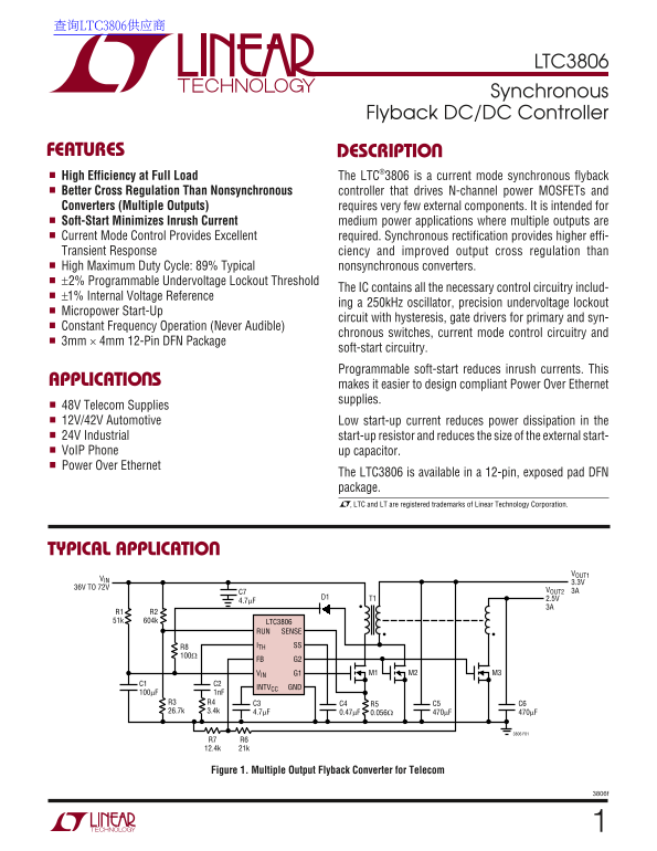
Figure 1. Multiple Output Flyback Converter for Telecom

Page Summary Contents For LINEAR LTC3806 Data Sheet Manual

Page 1 查询LTC3806供应商 LTC3806 Synchronous Flyback DC/DC Controller FEATURES DESCRIPTIO High Efficiency at Full Load The LTC®3806 is a current mode synchronous flyback Better Cross Regulation Than Nonsynchronou...
Page 2 LTC3806 ABSOLUTE MAXIMUM RATINGS PACKAGE/ORDER INFORMATION (Note 1) VIN Voltage 25V TOP VIEW ORDER PART INTVCC Voltage 8V NUMBER RUN SENSE INTVCC Output Current 50m A ITH NC LTC3806EDE G1, G2 Voltages...
Page 3 FB OL TA GE (V LTC3806 ELECTRICAL CHARACTERISTICS The ● denotes specifications which apply over the full operating temperature range, otherwise specifications are TA = 25°C. VIN = 10V, VRUN = 1.5V, un...
Page 4 TI (n s) SH UT DO OD E, (µ A) LTC3806 TYPICAL PERFOR A CE CHARACTERISTICS FR EQ UE NC (k Hz Shutdown Mode IQ Shutdown Mode IQ vs VIN vs Temperature Soft-Start Current vs Temperature TA = 25°C TI (n s)...
Page 5 SE NS PI CU RR EN (µ A) LTC3806 TYPICAL PERFOR A CE CHARACTERISTICS DR OP OU VO LT AG (V SENSE Pin Current vs Temperature INTVCC Load Regulation INTVCC Line Regulation 32.0 7.020 7.020 TA = 25°C IN TV...
Page 6 LTC3806 PI FU CTIO S RUN (Pin 1): The RUN pin provides the user with an INTVCC (Pin 6): The Internal 6.9V Regulator Output. The accurate means for sensing the input voltage and pro- gate drivers and c...
Page 7 LTC3806 BLOCK DIAGRA SLOPE COMPENSATION PWM SENSE LATCH INTVCC ITH C1 V-TO-I CURRENT LOGIC INTVCC RLOOPILOOP COMPARATOR G2 SOFT-START COMPARATOR RUN BIAS AND VREF C2 START-UP CONTROL REGULATOR GND INT...
Page 8 LTC3806 OPERATIO Main Control Loop the RUN pin below 1.139V, the chip is off and the input supply current is typically only 50µA. If the RUN pin is The LTC3806 is a constant frequency, current mode ab...
Page 9 LTC3806 APPLICATIO S I FOR ATIO INTVCC Regulator Bypassing and Operation If VIN is set to 10V, the power dissipation is: An internal voltage regulator produces the 6.9V supply PIC = 10 • 27m A = 270m ...
Page 10 LTC3806 APPLICATIO S I FOR ATIO Cross regulation and tracking between the master and slave Select a value for R7 less than or equal to 120k. Now outputs are impacted by transformer and secondary-side ...
Page 11 LTC3806 APPLICATIO S I FOR ATIO The rising threshold voltage on the RUN pin is equal to the For a 50% duty factor, this reduces to: internal reference voltage of 1.230V. The comparator has 91m V of hy...
Page 12 LTC3806 APPLICATIO S I FOR ATIO Some common secondary turns ratios: VOUT TURNS OUT IN 3.3 Input Power The maximum input power is: OUTKK =1 1.8 2.5 Eff IN 2.5 where POUTK is the maximum power supplied ...
Page 13 LTC3806 APPLICATIO S I FOR ATIO For a minimum input voltage of 36V, the largest duty factor cycle), and only about 70m V at a duty cycle of 92% due to is: slope compensation. Use Figure 4 and DMAX to ...
Page 14 LTC3806 APPLICATIO S I FOR ATIO characteristic. Refer to Application Note 19 for more The capacitance calculation begins with the maximum information. acceptable ripple voltage (expressed as a percent...
Page 15 LTC3806 APPLICATIO S I FOR ATIO Continuing our previous example the filter capacitor for LKG OUT MAX≥ output 1 needs: BV PK IN MAX where LLKG is the primary-side leakage inductance and CP ESR COUT is ...
Page 16 LTC3806 APPLICATIO S I FOR ATIO VIN ≅ VDS Compare TJ against your initial estimate for TJ and if necessary, recompute δ, power dissipations and TJ. Iter- MILLER EFFECT VGS ate as necessary. DEVICE UND...
Page 17 LTC3806 APPLICATIO S I FOR ATIO exceeds the maximum rating of the device, either choose 8. For optimum load regulation and true remote sensing, a higher voltage device or specify an avalanche-rated th...
Page 18 LTC3806 APPLICATIO S I FOR ATIO Table 1. Recommended Component Manufacturers VENDOR COMPONENTS TELEPHONE WEB ADDRESS AVX Capacitors 207-282-5111 avxcorp.com BH Electronics Transformers 952-894-9590 bh...
Page 19 LTC3806 PACKAGE DESCRIPTIO UE/DE Package 12-Lead Plastic DFN (4mm × 3mm) (Reference LTC DWG # 05-08-1695) (2 SIDES)2.20 ±0.05 PACKAGE OUTLINE 0.50 BSC 3.30 ±0.05 (2 SIDES) RECOMMENDED SOLDER PAD PITCH...
Page 20 LTC3806 TYPICAL APPLICATIO VOUT 12V VIN T1 B260A SMA 3.3µH SOD123 25V TO 60V XFMR EFD20 C1 GND 220n F VOUT ELEC C5 R1 R2 VOUT 232k 47k 3.3V 4V POSCAP Si4490 VOUT 2.5V LTC3806 R5 C11 RUN SENSE 0.033Ω 1...

Manual Details

Brand Linear
Pages 20
File Size 236.79 KB
Published June 15, 2026
5 views

Enter the captcha to get the download link:

captcha

Frequently Asked Questions

What package does the LTC3806 come in?

It is available in a 12-pin exposed pad DFN package measuring 3mm by 4mm.

What is the typical maximum duty cycle of the LTC3806?

The typical maximum duty cycle is 89%.

What are typical applications for the LTC3806?

It is used in 48V telecom, 12V/42V automotive, 24V industrial, VoIP phone and Power Over Ethernet supplies.