LINEAR LT3028 Data Sheet/Manual
Summary
The LT3028 is a micropower, dual Low Dropout Regulator designed for highly sensitive and battery-powered electronics. It delivers extremely low output noise (< 20µV) and ultra-low quiescent current (30µA/output), maintaining stability across a wide voltage range of 1.8V to 20V. Suitable for cellular phones and tracking supplies, the device features independent inputs for high flexibility, alongside robust protection against overcurrent and reverse battery operation.
Page 1 Text Content
查询LT3020IMS8供应商
LT3028
Dual 100m A/500m A Low Dropout, Low Noise,
Micropower Regulators with
Independent Inputs
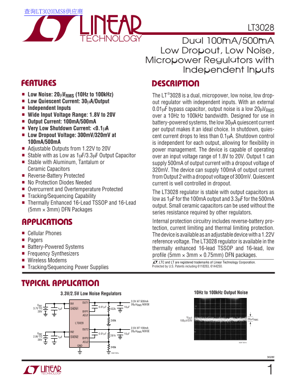
FEATURES DESCRIPTIO Low Noise: 20µVRMS (10Hz to 100k Hz) The LT®3028 is a dual, micropower, low noise, low drop- Low Quiescent Current: 30µA/Output out regulator with independent inputs. With an external Independent Inputs 0.01µF bypass capacitor, output noise is a low 20µVRMS Wide Input Voltage Range: 1.8V to 20V over a 10Hz to 100k Hz bandwidth. Designed for use in Output Current: 100m A/500m A battery-powered systems, the low 30µA quiescent current Very Low Shutdown Current: <0.1µA per output makes it an ideal choice. In shutdown, quies- Low Dropout Voltage: 300m V/320m V at cent current drops to less than 0.1µA. Shutdown control 100m A/500m A is independent for each output, allowing for flexibility in Adjustable Outputs from 1.22V to 20V power management. The device is capable of operating Stable with as Low as 1µF/3.3µF Output Capacitor over an input voltage range of 1.8V to 20V. Output 1 can Stable with Aluminum, Tantalum or supply 500m A of output current with a dropout voltage of Ceramic Capacitors 320m V. The device can supply 100m A of output current Reverse-Battery Protected from Output 2 with a dropout voltage of 300m V. Quiescent No Protection Diodes Needed current is well controlled in dropout. Overcurrent and Overtemperature Protected
The LT3028 regulator is stable with output capacitors as
Tracking/Sequencing Capability
low as 1µF for the 100m A output and 3.3µF for the 500m A
Thermally Enhanced 16-Lead TSSOP and 16-Lead
output. Small ceramic capacitors can be used without the
(5mm × 3mm) DFN Packages
series resistance required by other regulators. APPLICATIO S Internal protection circuitry includes reverse-battery pro- tection, current limiting and thermal limiting protection.
Cellular Phones
The device is available as an adjustable device with a 1.22V
Pagers
reference voltage. The LT3028 regulator is available in the
Battery-Powered Systems
thermally enhanced 16-lead TSSOP and 16-lead, low
Frequency Synthesizers
profile (5mm × 3mm × 0.75mm) DFN packages.
Wireless Modems
, LTC and LT are registered trademarks of Linear Technology Corporation. Protected by U.S. Patents including 6118263, 6144250.
Tracking/Sequencing Power Supplies
TYPICAL APPLICATIO
10Hz to 100k Hz Output Noise3.3V/2.5V Low Noise Regulators
3.3V AT 500m A
IN1VIN1 20µVRMS NOISE
3.7V TO 1µF SHDN1 422k 20V BYP1
20µVRMS
249k 100µV/DIV
LT3028
2.5V AT 100m A
IN2VIN2 20µVRMS NOISE
2.9V TO 1µF SHDN2
ADJ2 3028 TA01b GND
3028 TA01a
Page Summary Contents For LINEAR LT3028 Data Sheet/Manual
Manual Details
| Brand | Linear |
|---|---|
| Pages | 16 |
| File Size | 333.67 KB |
| Published | June 20, 2026 |
Enter the captcha to get the download link:

Frequently Asked Questions
What is the required capacitance for stable operation?
It is stable with Ceramic, Aluminum or Tantalum capacitors; low as 1µF is recommended for the 100mA output.
Is this regulator safe for battery-powered systems?
Yes, it offers very low quiescent current (< 30µA/output) and very low shutdown current (< 0.1µA).
What protection features does the LT3028 include?
It includes Overcurrent, Overtemperature, and Reverse-Battery Protection for enhanced safety.
What is the regulated output voltage range?
The adjustable outputs can operate within a wide voltage range of 1.22V to 20V.