LINEAR LTC3252 Data Sheet Manual
Summary
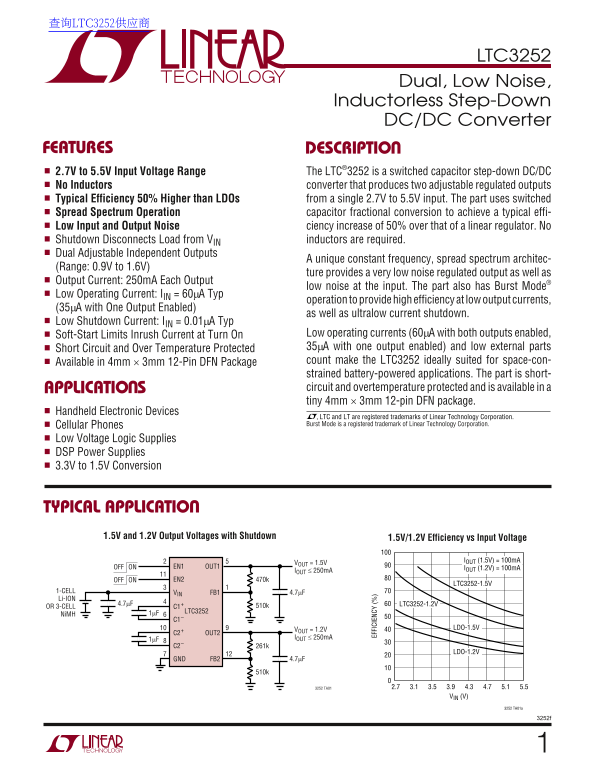
Harnessing low noise and high efficiency, this dual, inductorless step-down DC/DC converter provides two adjustable regulated outputs from a range of 2.7V to 5.5V. Ideal for battery-powered and space-constrained applications such as handheld devices, cellular phones, and DSP power supplies. This technical manual offers comprehensive details on electrical characteristics, spread spectrum operation, low quiescent current modes, and robust protection features, guiding system designers through optimal integration planning.
Page 1 Text Content
查询LTC3252供应商
LTC3252
Dual, Low Noise, Inductorless Step-Down DC/DC Converter
FEATURES DESCRIPTIO 2.7V to 5.5V Input Voltage Range The LTC®3252 is a switched capacitor step-down DC/DC No Inductors converter that produces two adjustable regulated outputs Typical Efficiency 50% Higher than LDOs from a single 2.7V to 5.5V input. The part uses switched
Spread Spectrum Operation capacitor fractional conversion to achieve a typical effi- Low Input and Output Noise ciency increase of 50% over that of a linear regulator. No Shutdown Disconnects Load from VIN inductors are required.
Dual Adjustable Independent Outputs
A unique constant frequency, spread spectrum architec-
(Range: 0.9V to 1.6V)
ture provides a very low noise regulated output as well as
Output Current: 250m A Each Output
low noise at the input. The part also has Burst Mode®
Low Operating Current: IIN = 60µA Typ
operation to provide high efficiency at low output currents,
(35µA with One Output Enabled)
as well as ultralow current shutdown.
Low Shutdown Current: IIN = 0.01µA Typ
Soft-Start Limits Inrush Current at Turn On Low operating currents (60µA with both outputs enabled, Short Circuit and Over Temperature Protected 35µA with one output enabled) and low external parts Available in 4mm × 3mm 12-Pin DFN Package count make the LTC3252 ideally suited for space-con-
EF FI CI EN CY strained battery-powered applications. The part is short-
APPLICATIO S circuit and overtemperature protected and is available in a tiny 4mm × 3mm 12-pin DFN package.
Handheld Electronic Devices
, LTC and LT are registered trademarks of Linear Technology Corporation. Cellular Phones Burst Mode is a registered trademark of Linear Technology Corporation.
Low Voltage Logic Supplies DSP Power Supplies 3.3V to 1.5V Conversion
TYPICAL APPLICATIO 1.5V and 1.2V Output Voltages with Shutdown 1.5V/1.2V Efficiency vs Input Voltage
IOUT (1.5V) = 100m A
VOUT = 1.5V
OFF ON EN1 OUT1 IOUT (1.2V) = 100m A
IOUT ≤ 250m A
ON EN2OFF 470k
LTC3252-1.5V
1-CELL VIN FB1 4.7µF Li-ION
4.7µF LTC3252-1.2V
OR 3-CELL C1+ 510k
LTC3252
Ni MH 1µF
LDO-1.5V
VOUT = 1.2V
C2+ OUT2
IOUT ≤ 250m A
LDO-1.2V
GND FB2 4.7µF
3252 TA01 2.7 3.1 3.5 3.9 4.3 4.7 5.1 5.5
VIN (V)
3252 TA01a
Page Summary Contents For LINEAR LTC3252 Data Sheet Manual
Manual Details
| Brand | Linear |
|---|---|
| Pages | 12 |
| File Size | 281.50 KB |
| Published | June 06, 2026 |
Enter the captcha to get the download link:

Frequently Asked Questions
What is the minimum input voltage for the LTC3252?
The operating range starts at 2.7V.
How does the LTC3252 achieve low noise output?
It uses a unique constant frequency, spread spectrum architecture.
What is the typical efficiency of this converter?
It offers a high typical efficiency through capacitor fractional conversion.
Is the product protected against overtemperature or short circuits?
Yes, it features inherent short circuit and overtemperature protection.