# A B C D E F G H I J K L M N O P Q R S T U V W X Y Z

LINEAR LT3437 Data Sheet / User Manual

Summary

The LT3437 is a high-efficiency, 200kHz monolithic buck switching regulator designed for robust power conversion in demanding environments. It features an ultra-wide input voltage range (3.3V to 60V, with protection up to 80V) and exceptionally low quiescent current (<1µA). This manual provides comprehensive technical details on its performance, covering transient response, burst mode operation, and soft-start capabilities. Ideal for engineers developing sophisticated solutions for Automotive, Industrial, Distributed Power Systems, and battery-powered electronics.
📄 Preview PAGE OF 24

Page 1 Text Content

查询LT3437供应商

LT3437

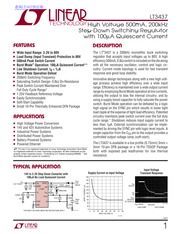
High Voltage 500m A, 200k Hz Step-Down Switching Regulator with 100µA Quiescent Current

FEATURES DESCRIPTIO

Wide Input Range: 3.3V to 60V The LT®3437 is a 200k Hz monolithic buck switching Load Dump (Input Transient) Protection to 80V regulator that accepts input voltages up to 80V. A high 500m A Peak Switch Current efficiency 500m A, 0.8Ω switch is included on the die along Burst Mode® Operation: 100µA Quiescent Current** with all the necessary oscillator, control and logic cir- Low Shutdown Current: IQ < 1µA cuitry. Current mode topology is used for fast transient Burst Mode Operation Defeat response and good loop stability.

200k Hz Switching Frequency

Innovative design techniques along with a new high volt-

Saturating Switch Design: 0.8Ω On-Resistance

age process achieve high efficiency over a wide input

SU PP LY UR RE NT (µ A)

Peak Switch Current Maintained Over

range. Efficiency is maintained over a wide output current

Full Duty Cycle Range*

range by employing Burst Mode operation at low currents,

1.25V Feedback Reference Voltage

utilizing the output to bias the internal circuitry, and by

Easily Synchronizable

using a supply boost capacitor to fully saturate the power

Soft-Start Capability

switch. Burst Mode operation can be defeated by a logic

Small 10-Pin Thermally Enhanced DFN Package

high signal on the SYNC pin which results in lower light load ripple at the expense of light load efficiency. Patented APPLICATIO S circuitry maintains peak switch current over the full duty cycle range.* Shutdown reduces input supply current to

High Voltage Power Conversion

less than 1µA. External synchronization can be imple-

14V and 42V Automotive Systems

mented by driving the SYNC pin with logic-level inputs. A

Industrial Power Systems

single capacitor from the CSS pin to the output provides a

Distributed Power Systems

controlled output voltage ramp (soft-start).

Battery-Powered Systems

The LT3437 is available in a low profile (0.75mm) 3mm ×

Powered Ethernet

3mm 10-pin DFN package or a 16-Pin TSSOP Package

, LTC and LT are registered trademarks of Linear Technology Corporation. Burst Mode is a registered trademark of Linear Technology Corporation. All other trademarks are the both with exposed pad leadframes for low thermal property of their respective owners. *Protected by U.S. Patents including 6498466. **See

Burst Mode Operation section for conditions. resistance.

TYPICAL APPLICATIO

Input Voltage

Supply Current vs Input Voltage Transient Response

14V to 3.3V Step-Down Converter with 100µA No Load Quiescent Current

VIN BOOST 3.3V

4.5V TO 80V* VIN

BAS21 20V/DIV

100V SHDN

CER LT3437 0.1µF

10MQ100N

CSSVC VIN

VBIAS

27p F 165k VOUT

100µF 20m V/DIV SYNC FB 6.3V AC COUPLED

TANT 3437 TA03

GND 100k 50ms/DIVIOUT 250m A

LOAD DUMP COLD CRANK

*FOR INPUT VOLTAGES ABOVE 60V RESTRICTIONS APPLY 3437 TA01

INPUT VOLTAGE (V)

3435 TA02

Page Summary Contents For LINEAR LT3437 Data Sheet / User Manual

Page 1 查询LT3437供应商 LT3437 High Voltage 500m A, 200k Hz Step-Down Switching Regulator with 100µA Quiescent Current FEATURES DESCRIPTIO Wide Input Range: 3.3V to 60V The LT®3437 is a 200k Hz monolithic buck sw...
Page 2 LT3437 ABSOLUTE AXI RATI GS (Note 1) Operating Junction Temperature Range VIN, SHDN, BIAS, SW Operating 60V LT3437EDD (Note 2) –40°C to 125°C VIN, SHDN 100ms Transient, &lt;15% Duty Cycle 80V LT3437ID...
Page 3 LT3437 ELECTRICAL CHARACTERISTICS The ● denotes the specifications which apply over the full operating temperature range, otherwise specifications are at TJ = 25°C. VIN = 12V, SHDN = 12V, BIAS = 5V, F...
Page 4 IN (µ A) VO LT AG (V EF FI CI EN CY LT3437 TYPICAL PERFOR A CE CHARACTERISTICS Efficiency and Power Loss Oscillator Frequency vs Load Current FB Voltage vs Temperature vs Temperature VIN = 12V VOUT = ...
Page 5 ON -T IM (n s) SU PP LY UR RE NT (µ A) SS (µ A) LT3437 TYPICAL PERFOR A CE CHARACTERISTICS Soft-Start Current Threshold Oscillator Frequency vs FB Voltage vs FB Voltage Switch On Voltage (VCESAT) SOFT...
Page 6 AX IM UM YN FR EQ UE NC (k Hz OU TP UT OL TA GE (V LT3437 TYPICAL PERFOR A CE CHARACTERISTICS Maximum Duty Cycle VC Switching Threshold Dropout Operation vs Temperature vs Temperature 94.5 0.6 VOUT = ...
Page 7 LT3437 PI FU CTIO S (DD/FE) SW (Pin 1/Pin 2): The SW pin is the emitter of the on-chip BIAS (Pin 6/Pin 10): The BIAS pin is used to improve power NPN switch. This pin is driven up to the input pin eff...
Page 8 LT3437 BLOCK DIAGRA INTERNAL REF SLOPE UNDERVOLTAGE LOCKOUT BIAS THERMAL 200k Hz SHUTDOWN CURRENT OSCILLATOR BOOST ANTISLOPE SHDN COMP SHDN SWITCH DRIVER COMP LATCH CIRCUITRY CSS BURST MODE SOFT-START...
Page 9 LT3437 APPLICATIO S I FOR ATIO FEEDBACK PIN FUNCTIONS Table 1 OUTPUT R1 OUTPUT The feedback (FB) pin on the LT3437 is used to set output VOLTAGE R2 NEAREST (1%) ERROR voltage and provide several overl...
Page 10 LT3437 APPLICATIO S I FOR ATIO function reduces input current surge by regulating switch cause the input voltage to swing above the DC level of input current via the VC pin to maintain a constant volt...
Page 11 LT3437 APPLICATIO S I FOR ATIO Table 2. Surface Mount Solid Tantalum Capacitor ESR may still affect the proper operation of the regulator. A and Ripple Current filter capacitor CF in parallel with the...
Page 12 LT3437 APPLICATIO S I FOR ATIO VOUT Discontinuous operation occurs when: 10m V/DIV 100µF TANTALUM ESR 75mΩ OUT IN OUT OUT DIS 10m V/DIV IN 100µF CERAMIC For VOUT = 5V, VIN = 8V and L = 68µH: VSW 10V/D...
Page 13 LT3437 APPLICATIO S I FOR ATIO more output current because they reduce peak current VIN = maximum input voltage seen by the LT3437 switch, which has a 0.5A limit. Higher f = switching frequency, 200k ...
Page 14 LT3437 APPLICATIO S I FOR ATIO A potential controllability problem could occur under SOFT-START short-circuit conditions. If the power supply output is For applications where [VIN/(VOUT + VF)] &gt;10 ...
Page 15 LT3437 APPLICATIO S I FOR ATIO current to the output capacitor followed by sleep periods VOUT = 3.3V where the output power is delivered to the load by the output capacitor. In addition, VIN and BIAS ...
Page 16 LT3437 APPLICATIO S I FOR ATIO OPTIONAL The use of so-called “ultrafast” recovery diodes is gener- ally not recommended. When operating in continuous mode, the reverse recovery time exhibited by “ultr...
Page 17 LT3437 APPLICATIO S I FOR ATIO below 2.4V, switching will be disabled. The undervoltage See the Typical Performance Characteristics section for lockout threshold doesn’t have any hysteresis and is gra...
Page 18 LT3437 APPLICATIO S I FOR ATIO inductance of approximately 25n H/inch. At switch off, this The VC and FB components should be kept as far away as parasitic inductance produces a flyback spike across t...
Page 19 LT3437 APPLICATIO S I FOR ATIO (tr + tf + t IR + t IF) that AC switching loss is proportional to both operating frequency and output current. The majority of AC switch- tr = (VIN/0.6)ns ing loss is al...
Page 20 LT3437 APPLICATIO S I FOR ATIO FREQUENCY COMPENSATION A zero can be added into the loop by placing a resistor (RC) at the VC pin in series with the compensation capacitor, CC, Before starting on the t...
Page 21 LT3437 APPLICATIO S I FOR ATIO LT3437 CURRENT MODE POWER STAGE OUTPUT gm = 1 R1 CFB gm = 650µ ERROR AMP R2 ESR 1.6MRC PHASE (DEG) 1.25V GA IN (d B) CF COUT Figure 10. Model for Loop Response VOUT = 3....
Page 22 LT3437 PACKAGE DESCRIPTIO DD Package 10-Lead Plastic DFN (3mm × 3mm) (Reference LTC DWG # 05-08-1699) (2 SIDES)2.15 ±0.05 PACKAGE OUTLINE 0.50 BSC 2.38 ±0.05 (2 SIDES) RECOMMENDED SOLDER PAD PITCH AND...
Page 23 LT3437 PACKAGE DESCRIPTIO FE Package 16-Lead Plastic TSSOP (4.4mm) (Reference LTC DWG # 05-08-1663) Exposed Pad Variation BC SEE NOTE 4 2.94 (.252) (.116) 0.45 ±0.05 BSC 0.65 BSC 2RECOMMENDED SOLDER P...
Page 24 POW ER LOSS (m LT3437 TYPICAL APPLICATIO 14V to 3.3V Step-Down Converter with Supply Current vs Efficiency and Power Loss 100µA No Load Quiescent Current Input Voltage vs Load Current VOUT VIN = 12V V...

Manual Details

Brand Linear
Pages 24
File Size 508.14 KB
Published June 05, 2026
59 views

Enter the captcha to get the download link:

captcha

Frequently Asked Questions

What are the input voltage limits for the LT3437 regulator?

It functions with a wide input range from 3.3V up to 60V, accepting inputs even up to 80V.

How is efficiency maintained during light load conditions?

Burst Mode Operation allows the device to maintain high efficiency over a wide output current full duty cycle range.

Can an external circuit synchronize with this regulator's switching frequency?

Yes, external synchronization can be accomplished by driving the SYNC pin on the chip.

Does the LT3437 protect against sudden input voltage spikes?

It includes High Load Dump (Input Transient) Protection up to 80V.