# A B C D E F G H I J K L M N O P Q R S T U V W X Y Z

LINEAR LTC2446 LTC2447 Data Sheet User Manual

Summary

These 24-bit, high-speed $\Delta\Sigma$ Analog-to-Digital Converters are designed for sophisticated multiple ratiometric measurement systems. Featuring up to eight channels and five selectable differential reference inputs, they precisely digitize diverse sensors (such as RTDs, bridges, and thermocouples) with exceptional low noise and variable speed control. This comprehensive manual details the electrical characteristics, pinout, and optimal application methods necessary for builders of weight scales, gas chromatographs, and advanced instrumentation requiring high accuracy up to 8kHz.
📄 Preview PAGE OF 28

Page 1 Text Content

查询LTC2445IUHF供应商

LTC2446/LTC2447 24-Bit High Speed 8-Channel ∆Σ ADCs with

Selectable Multiple Reference Inputs

FEATURES DESCRIPTIO

Five Selectable Differential Reference Inputs The LTC®2446/LTC2447 4-terminal switching enables

Four Differential/Eight Single-Ended Inputs multiplexed ratiometric measurements. Four sets of se- 4-Way MUX for Multiple Ratiometric lectable differential inputs coupled with four sets of differ- Measurements ential reference inputs allow multiple RTDs, bridges and Up to 8k Hz Output Rate

other sensors to be digitized by a single converter. A fifth

Up to 4k Hz Multiplexing Rate

differential reference input can be selected for any input

Selectable Speed/Resolution:

channel not requiring ratiometric measurements (ther-

2µVRMS Noise at 1.76k Hz Output Rate

mocouples, voltages, current sense, etc.). The flexible

200n VRMS Noise at 13.8Hz Output Rate with

input multiplexer allows single-ended or differential in-

Simultaneous 50/60Hz Rejection

puts coupled with a slaved reference input or a universal

Guaranteed Modulator Stability and Lock-Up

reference input.

Immunity for any Input and Reference Conditions 0.0005% INL, No Missing Codes

A proprietary delta-sigma architecture results in absolute

Autosleep Enables 20µA Operation at 6.9Hz

accuracy (offset, full-scale, linearity) of 15ppm, noise as

<5µV Offset (4.5V < VCC < 5.5V, –40°C to 85°C)

low as 200n VRMS and speeds as high as 8k Hz. Through a

Differential Input and Differential Reference with

RM NO IS (µ V) simple 4-wire interface, ten speed/resolution combina-

GND to VCC Common Mode Range

tions can be selected. The first conversion following a

No Latency Mode, Each Conversion is Accurate Even

speed, resolution, channel change or reference change is

After a New Channel is Selected

valid since there is no settling time between conversions,

Internal Oscillator—No External Components

LTC2447 Includes MUXOUT/ADCIN for External enabling scan rates of up to 4k Hz. Additionally, a 2x mode Buffering or Gain can be selected for any speed-enabling output rates up to Tiny QFN 5mm x 7mm Package 8k Hz with one cycle of latency. , LTC and LT are registered trademarks of Linear Technology Corporation. APPLICATIO S Protected by U.S. Patents, including 6140950, 6169506, 6208279, 6411242, 6639526

Flow Weight Scales Pressure Direct Temperature Measurement Gas Chromatography

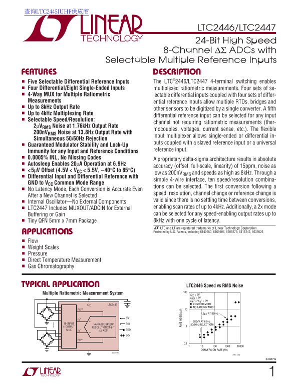
TYPICAL APPLICATIO LTC2446 Speed vs RMS Noise Multiple Ratiometric Measurement System VCC = 5V

VREF = 5V + = VIN – = 0V VIN VCC LTC2446 2x SPEED MODE NO LATENCY MODE

2.8µV AT 880Hz

280n V AT 6.9Hz

19-INPUT VARIABLE SPEED/ SDI

(50/60Hz REJECTION)

4-OUTPUT RESOLUTION 24-BIT

MUX IN– ∆Σ ADC SDO

CONVERSION RATE (Hz)

24467 TA01

24467 TA02

24467fa

Page Summary Contents For LINEAR LTC2446 LTC2447 Data Sheet User Manual

Page 1 查询LTC2445IUHF供应商 LTC2446/LTC2447 24-Bit High Speed 8-Channel ∆Σ ADCs with Selectable Multiple Reference Inputs FEATURES DESCRIPTIO Five Selectable Differential Reference Inputs The LTC®2446/LTC2447 4-...
Page 2 LTC2446/LTC2447 ABSOLUTE AXI RATI GS (Notes 1, 2) Supply Voltage (VCC) to GND.......................–0.3V to 6V Digital Output Voltage to GND –0.3V to (VCC + 0.3V) Analog Input Pins Voltage Operating ...
Page 3 LTC2446/LTC2447 ELECTRICAL CHARACTERISTICS The ● denotes specifications which apply over the full operating temperature range, otherwise specifications are at TA = 25°C. (Notes 3, 4) PARAMETER CONDITI...
Page 4 LTC2446/LTC2447 DIGITAL I PUTS A D DIGITAL OUTPUTS The ● denotes specifications which apply over the full operating temperature range, otherwise specifications are at TA = 25°C. (Note 3) SYMBOL PARAME...
Page 5 LTC2446/LTC2447 TI G CHARACTERISTICS The ● denotes specifications which apply over the full operating temperature range, otherwise specifications are at TA = 25°C. (Note 3) SYMBOL PARAMETER CONDITIONS...
Page 6 LTC2446/LTC2447 PI FU CTIO – 0.3V to VCC + 0.3V. Within these limits, the two selected contains an enable bit which determines if a new channel/ inputs (IN+ and IN–) provide a bipolar input range (VIN...
Page 7 LTC2446/LTC2447 FU CTIO AL BLOCK DIAGRA VREF01 INTERNAL OSCILLATOR VREF01 AUTOCALIBRATION FO VREF67 AND CONTROL (INT/EXT) VREF67 VREFG PU T/ RE FE RE NC UX VREFG CH0 CH1 DIFFERENTIAL SDI 3RD ORDER IN–...
Page 8 LTC2446/LTC2447 APPLICATIO S I FOR ATIO sleep state. While in this sleep state, power consumption below approximately 2.2V. This feature guarantees the is reduced below 10µA. The part remains in the s...
Page 9 LTC2446/LTC2447 APPLICATIO S I FOR ATIO convert the bipolar differential input signal, VIN = IN+ – Bit 31 (first output bit) is the end of conversion (EOC) IN– (where IN+ and IN– are the selected inpu...
Page 10 LTC2446/LTC2447 APPLICATIO S I FOR ATIO CS SDI EN SGL GLBL A1 A0 OSR3 OSR2 OSR1 OSR0 TWOXODD BIT 31 BIT 30 BIT 29 BIT 28 BIT 27 BIT 26 BIT 25 BIT 24 BIT 23 BIT 22 BIT 21 BIT 20 BIT 19 BIT 0 Hi-Z SDO E...
Page 11 LTC2446/LTC2447 APPLICATIO S I FOR ATIO Serial Clock Input/Output (SCK) Initially, after powering up, the device performs a conver- +, REF– = sion with IN+ = CH0, IN– = CH1, REF+ = VREF01 The serial c...
Page 12 LTC2446/LTC2447 APPLICATIO S I FOR ATIO Table 3. Channel Selection for the LTC2446/LTC2447 MUX ADDRESS CHANNEL INPUT REFERENCE INPUT ODD/ SGL SIGN GLBL A1 A0 COM 01+ 01– 23+ 23– 45+ 45– 67+ 67– G+ G– ...
Page 13 LTC2446/LTC2447 APPLICATIO S I FOR ATIO Table 4. LTC2446/LTC2447 Speed/Resolution Selection CONVERSION RATE INTERNAL EXTERNAL RMS RMS 9MHz 10.24MHz NOISE NOISE ENOB ENOB OSR3 OSR2 OSR1 OSR0 TWOX CLOCK...
Page 14 LTC2446/LTC2447 APPLICATIO S I FOR ATIO Speed Multiplier Mode the conversion cycle (just prior to the data output cycle) for auto calibration. The time required to read the conver- In addition to sele...
Page 15 LTC2446/LTC2447 APPLICATIO S I FOR ATIO External Serial Clock, Single Cycle Operation When the device is in the sleep state (EOC = 0), its (SPI/MICROWIRE Compatible) conversion result is held in an in...
Page 16 LTC2446/LTC2447 APPLICATIO S I FOR ATIO As described above, CS may be pulled LOW at any time in output sequence is aborted prior to the 13th rising edge of order to monitor the conversion status on th...
Page 17 LTC2446/LTC2447 APPLICATIO S I FOR ATIO External Serial Clock, 3-Wire I/O indicating the conversion result is ready. EOC = 1 (BUSY = 1) while the conversion is in progress and This timing mode utilize...
Page 18 LTC2446/LTC2447 APPLICATIO S I FOR ATIO Internal Serial Clock, Single Cycle Operation sion and goes LOW at the conclusion. It remains LOW until the result is read from the device. This timing mode use...
Page 19 LTC2446/LTC2447 APPLICATIO S I FOR ATIO If CS remains LOW longer than t EOCtest, the first rising of SCK, see Figure 8. On the rising edge of CS, the device edge of SCK will occur and the conversion r...
Page 20 LTC2446/LTC2447 APPLICATIO S I FOR ATIO Internal Serial Clock, 3-Wire I/O, device has entered the low power sleep state. The part Continuous Conversion remains in the sleep state a minimum amount of t...
Page 21 LTC2446/LTC2447 NO RM AL OD RE JE CT IO (d B) NO RM AL OD RE JE CT IO (d B) APPLICATIO S I FOR ATIO Normal Mode Rejection and Antialiasing Table 6. OSR vs Notch Frequency (f N) (with Internal Oscillat...
Page 22 LTC2446/LTC2447 NO RM AL OD RE JE CT IO (d B) APPLICATIO S I FOR ATIO offset and full-scale performance remain unchanged as 4.5V TO 5.5V does the first multiple of f S. The sample rate f S and NULL f ...
Page 23 LTC2446/LTC2447 APPLICATIO S I FOR ATIO VREF 10µF LTC2446 VREFG VREFO1 VREFO1 VREF23 RATIOMETRIC VREF23 IN+ CH2 VARIABLE SPEED SDI RESOLUTION IN– 24-BIT ∆Σ ADC SDO CH4 VREF45 BRIDGE CH5 VREF45 CH6 CH7...
Page 24 LTC2446/LTC2447 APPLICATIO S I FOR ATIO Table 7. Performance vs Over-Sample Ratio MAXIMUM FIRST NOTCH EFFECTIVE –3d B CONVERSION RATE FREQUENCY NOISE BW POINT (Hz) OVER- SAMPLE *RMS *RMS ENOB INTERNAL...
Page 25 LTC2446/LTC2447 APPLICATIO S I FOR ATIO Automatic Offset Calibration of External attenuates sampling glitches from the LTC2447 ADCIN Buffers/Amplifiers terminal, allowing it to achieve full performanc...
Page 26 LTC2446/LTC2447 APPLICATIO S I FOR ATIO Figure 18a is a standard 350Ω, voltage excited strain gauge The LTC2446 multiplexes rail-to-rail inputs directly to the with sense wires for the excitation volt...
Page 27 LTC2446/LTC2447 PACKAGE DESCRIPTIO UHF Package 38-Lead Plastic QFN (5mm × 7mm) (Reference LTC DWG # 05-08-1701) 5.50 ± 0.05 (2 SIDES) 4.10 ± 0.05 (2 SIDES) 3.15 ± 0.05 (2 SIDES) PACKAGE OUTLINE 0.25 ±...
Page 28 LTC2446/LTC2447 APPLICATIO S I FOR ATIO FUJIKURA FPM-120PG VREF01 (4k TO 6k IMPEDANCE) CH3+– +– FULL-SCALE OUTPUT = 60m V TO 140m V 350Ω CH0 LOAD CELL CH2 FULL-SCALE OUTPUT = 10m V VREF23 SELECT FOR V...

Manual Details

Brand Linear
Pages 28
File Size 285.66 KB
Published June 18, 2026
5 views

Enter the captcha to get the download link:

captcha

Frequently Asked Questions

What is the maximum number of inputs I can measure?

The device supports up to eight differential or sixteen single-ended inputs for multiplexed ratiometric measurements.

Does measurement accuracy drop after changing channels or reference inputs?

No, there is no settling time between conversions; each conversion remains accurate immediately after a channel or reference change.

What are the measured noise levels and maximum rate?

The ADC features high precision with ultra-low noise, such as 2µV at 1.76kHz or 200nV at 13.8Hz. It can output rates up to 8kHz.

How do I determine the correct operating temperature range for my model?

Industrial versions ('I' suffix) operate from –40°C to 85°C, while commercial versions ('C' suffix) function between 0°C and 70°C.