# A B C D E F G H I J K L M N O P Q R S T U V W X Y Z

LINEAR LTC3425 Data Sheet User Manual

Summary

Technical datasheet for Linear Technology LTC3425 5A, 8MHz, 4-phase synchronous step-up DC/DC converter capable of operation below 1V input. Features four N-channel MOSFET switches and four P-channel synchronous rectifiers for effective RDS(ON) of 0.045Ω and 0.05Ω respectively, 4-phase operation greatly reducing peak inductor currents and capacitor ripple current while increasing effective switching frequency to minimize inductor and capacitor sizes. Provides true output disconnect eliminating i
📄 Preview PAGE OF 24

Page 1 Text Content

查询LT3425供应商

LTC3425

5A, 8MHz, 4-Phase Synchronous Step-Up DC/DC Converter

FEATURES DESCRIPTIO High Efficiency: Up to 95% The LTC®3425 is a synchronous, 4-phase boost converter Up to 3A Continuous Output Current with output disconnect capable of operation below 1V

4-Phase Operation for Low Output Ripple input. It includes four N-channel MOSFET switches and and Tiny Solution Size four P-channel synchronous rectifiers for an effective Output Disconnect and Inrush Current Limiting RDS(ON) of 0.045Ω and 0.05Ω, respectively. 4-phase

Very Low Quiescent Current: 12µA operation greatly reduces peak inductor currents, and 0.5V to 4.5V Input Range capacitor ripple current, and increases effective switching 2.4V to 5.25V Adjustable Output Voltage frequency, minimizing inductor and capacitor sizes. True Adjustable Current Limit output disconnect eliminates inrush current and allows Adjustable, Fixed Frequency Operation from zero load current in shutdown. External Schottky diodes 100k Hz to 2MHz per Phase are not required in most applications (VOUT < 4.3V). Power Synchronizable Oscillator with Sync Output saving Burst Mode operation can be user controlled or left Internal Synchronous Rectifiers in automatic mode. Manual or Automatic Burst Mode® Operation

Other features include 1µA shutdown current, program-

Power Good Comparator

mable frequency with sync in and out, programmable

<1µA Shutdown Current

soft-start, antiringing control, thermal shutdown, adjust-

Antiringing Control

able current limit, reference output and power good

EF FI CI EN CY

5mm × 5mm Thermally Enhanced QFN Package

comparator.

APPLICATIO S The LTC3425 is available in a small, thermally enhanced

32-pin QFN package.

Handheld Computers

, LTC and LT are registered trademarks of Linear Technology Corporation.

Point-of-Load Regulators Burst Mode is a registered trademark of Linear Technology Corporation. 3.3V to 5V Conversion

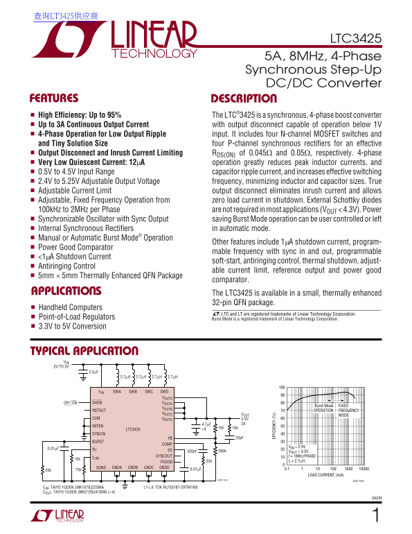
TYPICAL APPLICATIO VIN 2V TO 3V

VIN SWA SWB SWC SWD

VOUTS

SHDNOFF ON VOUTA

Burst Mode FIXED

VOUTB

REFOUT OPERATION FREQUENCY

VOUTC VOUT

CCM VOUTD 3.3V

REFEN

LTC3425

SYNCIN

FB 22p F

BURST

VIN = 2.4V

0.01µF RT

SS 330p F 590k VOUT = 3.3V ILIM SYNCOUT f = 1MHz/PHASE

PGOOD 33k L = 2.7µH

SGND GNDA GNDB GNDC GNDD

LOAD CURRENT (m A)

3425 TA01 3425 TA02

CIN: TAIYO YUDEN JMK107BJ225MA L1-L4: TDK RLF5018T-2R7M1R8

COUT: TAIYO YUDEN JMK212BJ475MG (×4)

Page Summary Contents For LINEAR LTC3425 Data Sheet User Manual

Page 1 查询LT3425供应商 LTC3425 5A, 8MHz, 4-Phase Synchronous Step-Up DC/DC Converter FEATURES DESCRIPTIO High Efficiency: Up to 95% The LTC®3425 is a synchronous, 4-phase boost converter Up to 3A Continuous Outp...
Page 2 LTC3425 ABSOLUTE AXI RATI GS PACKAGE/ORDER I FOR ATIO (Note 1) VIN Voltage –0.3V to 6V TOP VIEW SWA-D Voltages ..........................................–0.3V to 6V VOUTA-D, VOUTS Voltages...............
Page 3 LTC3425 ELECTRICAL CHARACTERISTICS The ● denotes the specifications which apply over the full operating temperature range, otherwise specifications are at TA = 25°C. VIN = 1.2V, VOUT = 3.3V, RT = 15k,...
Page 4 LTC3425 TYPICAL PERFOR A CE CHARACTERISTICS SW Pin and Inductor Current in Discontinous Mode. Antiring SWA, SWB, SWC, SWD Circuit Eliminates High Frequency at 1MHz/Phase SW Pin and Oscillator SYNCOUT ...
Page 5 FR EQ UE NC (M Hz EF FI CI EN CY EF FI CI EN CY LTC3425 TYPICAL PERFOR A CE CHARACTERISTICS Converter Efficiency Converter Efficiency Converter Efficiency for 2-, 3- and for VOUT = 3.3V for VOUT = 5V ...
Page 6 ST AR VO LT AG (V LO AD UR RE NT (m A) OU TP UT UR RE NT (m A) LTC3425 TYPICAL PERFOR A CE CHARACTERISTICS Maximum Output Current Maximum Start-Up Load vs VIN Automatic Burst Mode Current in Burst Mod...
Page 7 LTC3425 TYPICAL PERFOR A CE CHARACTERISTICS QU IE SC EN CU RR EN (µ A) Peak Current Limit Oscillator Frequency Feedback Voltage vs Temperature vs Temperature vs Temperature PE AK IM (N OR AL IZ ED ) (...
Page 8 LTC3425 PI FU CTIO GNDA–D (Pins 1, 2, 7, 8, 17, 18, 23, 24): Power Ground COMP (Pin 13): Error Amp Output. A frequency compen- for the IC and the Four Internal N-channel MOSFETs. sation network is con...
Page 9 LTC3425 PI FU CTIO ILIM (Pin 27): Current Limit Adjust Pin. Connect a resistor SYNCIN (Pin 30): Oscillator Synchronization Pin. A clock from ILIM to SGND to set the peak current limit threshold pulse ...
Page 10 LTC3425 BLOCK DIAGRA 1V TO 4.5V VIN SWA SWB SWC SWD 1 OF 4 VOUTA 2.5V TO 5.25V VOUTB ANTIRING VOUTC ENABLE VOUTD PWM LOGIC MODE CONTROL AND CCM DRIVERS DIVIDER 4-PHASE VOUTS SLOPE RT28 IOSC PGOOD +OSC...
Page 11 LTC3425 OPERATIO DETAILED DESCRIPTION SINGLE PHASE The LTC3425 provides high efficiency, low noise power for high current boost applications such as cellular phones and PDAs. The true output disconnec...
Page 12 LTC3425 OPERATIO SWITCH A VOLTAGE SWITCH B VOLTAGE SWITCH C VOLTAGE SWITCH D VOLTAGE INDUCTOR A CURRENT INDUCTOR B CURRENT INDUCTOR C CURRENT INDUCTOR D CURRENT INPUT CURRENT RECTIFIER A CURRENT RECTI...
Page 13 LTC3425 OPERATIO SWITCH A VOLTAGE SWITCH B VOLTAGE SWITCH C VOLTAGE SWITCH D VOLTAGE INDUCTOR A CURRENT INDUCTOR B CURRENT INDUCTOR C CURRENT INDUCTOR D CURRENT INPUT CURRENT RECTIFIER A CURRENT RECTI...
Page 14 LTC3425 EF FI CI EN CY OPERATIO TA = 25°C VIN = 2.4V VOUT = 3.3V 1MHz/PHASE SWITCH 4 PHASE where f OSC is in MHz and RT is in kΩ. 3 PHASE2 PHASE The oscillator can be synchronized with an external clo...
Page 15 LTC3425 OPERATIO Current Limit: The programmable current limit circuit sets the soft-start capacitor will be reset. The part will be the maximum peak current in the NMOS switches. The enabled again wh...
Page 16 LTC3425 OPERATIO a heavy load is suddenly applied to the converter after to sink up to 2m A. Note that Burst Mode operation is being in Burst Mode operation for an extended period of inhibited during ...
Page 17 LTC3425 APPLICATIO S I FOR ATIO The inductor current ripple is typically set to 20% to 40% of the maximum inductor current. CSS L4 For high efficiency, choose an inductor with high fre- quency core ma...
Page 18 LTC3425 APPLICATIO S I FOR ATIO The ESR (equivalent series resistance) is usually the most voltage from exceeding its maximum rating during the dominant factor for ripple in most power converters. The...
Page 19 LTC3425 APPLICATIO S I FOR ATIO VIN 3.3V D2 CS 0.47µF D3 ×2 VIN SWA SWB SWC SWD Q1 VOUTS SHDN VOUTA VOUTB REFOUT VOUTC VOUT CCM VOUTD 5V COUT CBULK REFEN 4.7µF R2 R4 150µF LTC3425 SYNCIN VOUT BURST RT...
Page 20 LTC3425 APPLICATIO S I FOR ATIO modulator control to output DC gain, and the error amp open-loop gain gives the DC gain of the system: LRHPZ OUT At heavy loads this gain increase with phase lag can oc...
Page 21 LTC3425 TYPICAL APPLICATIO S Single or Dual Cell to 3.3V Boost with Automatic Burst Mode Operation VIN = 1.1V TO 3V CIN 2.2µF L1 L2 L3 L4 VIN SWA SWB SWC SWD VOUTS R5 SHDN VOUTA 10k VOUTB C1 REFOUT VO...
Page 22 LTC3425 TYPICAL APPLICATIO S Application with User Commanded Burst Mode Operation and Buffered Reference Output Enabled VIN = 1.8V TO 3V CIN 2.2µF L1 L2 L3 L4 VIN SWA SWB SWC SWD VOUTS R4 SHDN VOUTA 1...
Page 23 LTC3425 PACKAGE DESCRIPTIO UH Package 32-Lead Plastic QFN (5mm × 5mm) (Reference LTC DWG # 05-08-1693) 3.45 ±0.05 (4 SIDES) PACKAGE OUTLINE 0.23 ± 0.05 0.50 BSC RECOMMENDED SOLDER PAD LAYOUT BOTTOM VI...
Page 24 LTC3425 TYPICAL APPLICATIO 10MHz, High Current, Very Low Profile, 8-Phase Converter Using Two LTC3425s Operating in Fixed Frequency Mode with Forced CCM (Max Component Height = 1.6mm) VIN 2.5V CIN1 CI...

Manual Details

Brand Linear
Pages 24
File Size 301.74 KB
Published June 18, 2026
4 views

Enter the captcha to get the download link:

captcha

Frequently Asked Questions

What is the maximum continuous output current?

The device can provide up to 3A of continuous output current.

How efficient is the LTC3425 converter?

It provides high efficiency, achieving up to 95% efficiency in typical operation.

Are external Schottky diodes required for most applications?

No, external Schottky diodes are generally not needed in most applications where V < 4.3V.

What is the usable input voltage range?

The device supports a wide power input range from 2V to 6V (operating ambient temperature range).

Does it have adjustable operation modes?

Yes, it features adjustable output voltage and allows for both fixed and variable frequency operation.