# A B C D E F G H I J K L M N O P Q R S T U V W X Y Z

LINEAR LTC2495 Data Sheet User Manual

Summary

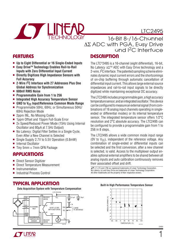
The LTC2495 is a high-performance 16-bit Delta-Sigma Analog-to-Digital Converter (ADC) featuring up to eight differential or sixteen single-ended inputs. This chip provides advanced signal acquisition capabilities using Easy Drive technology, ensuring maximum accuracy and low noise across wide common-mode ranges. The device includes programmable gain, an integrated temperature sensor, and a versatile I²C interface. Its manual details comprehensive features for engineers designing systems requiring precise measurement in diverse applications, from industrial control to data logging.
📄 Preview PAGE OF 32

Page 1 Text Content

LTC2495

16-Bit 8-/16-Channel

ΔΣ ADC with PGA, Easy Drive

and I2C Interface

FEATURES DESCRIPTION ■ Up to Eight Differential or 16 Single-Ended Inputs

The LTC®2495 is a 16-channel (eight differential), 16-bit,

■ Easy Drive TM Technology Enables Rail-to-Rail

No Latency ΔΣTM ADC with Easy Drive technology and a

Inputs with Zero Differential Input Current 2-wire, I2C interface. The patented sampling scheme elimi- ■ Directly Digitizes High Impedance Sensors with

nates dynamic input current errors and the shortcomings

Full Accuracy of on-chip buffering through automatic cancellation of ■ 2-Wire I2C Interface with 27 Addresses Plus One

differential input current. This allows large external source

Global Address for Synchronization impedances and rail-to-rail input signals to be directly ■ 600n V RMS Noise

digitized while maintaining exceptional DC accuracy.

■ Programmable Gain from 1 to 256

The LTC2495 includes programmable gain, a high accuracy

■ Integrated High Accuracy Temperature Sensor

temperature sensor, and an integrated oscillator. This device

■ GND to VCC Input/Reference Common Mode Range

can be confi gured to measure an external signal (from com-

■ Programmable 50Hz, 60Hz, or Simultaneous 50Hz/ AB SO LU TE RR OR (° C)

binations of 16 analog input channels operating in single-

60Hz Rejection Mode

ended or differential modes) or its internal temperature

■ 2ppm INL, No Missing Codes

sensor. The integrated temperature sensor offers 1/2°C

■ 1ppm Offset and 15ppm Full-Scale Error

resolution and 2°C absolute accuracy. The LTC2495 can

■ 2x Speed/Reduced Power Mode (15Hz Using Internal

be confi gured to provide a programmable gain from 1 to

Oscillator and 80µA at 7.5Hz Output)

256 in 8 steps.

■ No Latency: Digital Filter Settles in a Single Cycle,

Even After a New Channel is Selected The LTC2495 allows a wide common mode input range

■ Single Supply 2.7V to 5.5V Operation (0.8m W) (0V to VCC), independent of the reference voltage. Any ■ Internal Oscillator combination of single-ended or differential inputs can ■ Tiny 5mm × 7mm QFN Package be selected and the fi rst conversion, after a new channel

is selected, is valid. Access to the multiplexer output en-

APPLICATIONS ables optional external amplifi ers to be shared between all

analog inputs and auto calibration continuously removes

■ Direct Sensor Digitizer

their associated offset and drift.

■ Direct Temperature Measurement

, LT, LTC and LTM are registered trademarks of Linear Technology Corporation.

■ Instrumentation

No Latency ∆Σ and Easy Drive are trademarks of Linear Technology Corporation. ■ Industrial Process Control All other trademarks are the property of their respective owners.

TYPICAL APPLICATION

Built-In High Performance Temperature Sensor

Data Acquisition System with Temperature Compensation

2.7V TO 5.5V

CH0 VCCMUXOUT/ 0.1µF 10µF

CH1 ADCIN

REF+ 1.7k

CH7 IN+ 16-CHANNEL SDA –1 CH8 16-BIT ∆Σ ADC 2-WIRE

WITH EASY DRIVE I2C INTERFACE

SCL –2

CH15 –3

TEMPERATURE FO

MUXOUT/

SENSOR OSC –55 –30 –5

ADCIN

TEMPERATURE (°C)

2495 TA01 2495 TA02

Page Summary Contents For LINEAR LTC2495 Data Sheet User Manual

Page 1 LTC2495 16-Bit 8-/16-Channel ΔΣ ADC with PGA, Easy Drive and I2C Interface FEATURES DESCRIPTION ■ Up to Eight Differential or 16 Single-Ended Inputs The LTC®2495 is a 16-channel (eight differential), ...
Page 2 LTC2495 PACKAGE/ORDER INFORMATIONABSOLUTE MAXIMUM RATINGS (Notes 1, 2) TOP VIEW Supply Voltage (VCC) ................................... –0.3V to 6V Analog Input Voltage (CH0-CH15, COM) .................
Page 3 LTC2495 ELECTRICAL CHARACTERISTICS (NORMAL SPEED) The ● denotes the specifi cations which apply over the full operating temperature range, otherwise specifi cations are at TA = 25°C. (Notes 3, 4) PARA...
Page 4 LTC2495 ANALOG INPUT AND REFERENCE The ● denotes the specifi cations which apply over the full operating temperature range, otherwise specifi cations are at TA = 25°C. (Note 3) SYMBOL PARAMETER CONDIT...
Page 5 LTC2495 POWER REQUIREMENTS The ● denotes the specifi cations which apply over the full operating temperature range, otherwise specifi cations are at TA = 25°C. (Note 3) SYMBOL PARAMETER CONDITIONS MIN...
Page 6 NU BE OF EA DI NG TU (p pm f V IN (p pm f V RE F) RE F) LTC2495 TYPICAL PERFORMANCE CHARACTERISTICS Integral Nonlinearity Integral Nonlinearity Integral Nonlinearity (VCC = 5V, VREF = 5V) (VCC = 5V, V...
Page 7 OF FS ET RR OR (p pm f V RM NO IS (µ V) RM NO IS (µ V) RE F) LTC2495 TYPICAL PERFORMANCE CHARACTERISTICS RMS Noise vs Input Differential Voltage RMS Noise vs VIN(CM) RMS Noise vs Temperature (TA) 1.0 ...
Page 8 RE JE CT IO (d B) SL EE OD CU RR EN (µ A) FR EQ UE NC (k Hz LTC2495 TYPICAL PERFORMANCE CHARACTERISTICS On-Chip Oscillator Frequency On-Chip Oscillator Frequency vs Temperature vs VCC PSRR vs Frequenc...
Page 9 RM NO IS (µ V) IN (p pm EF OF FS ET RR OR (µ V) LTC2495 TYPICAL PERFORMANCE CHARACTERISTICS Integral Nonlinearity (2x Speed Integral Nonlinearity (2x Speed Noise Histogram Mode; VCC = 5V, VREF = 2.5V)...
Page 10 RE JE CT IO (d B) LTC2495 TYPICAL PERFORMANCE CHARACTERISTICS PSRR vs Frequency at VCC PSRR vs Frequency at VCC PSRR vs Frequency at VCC (2x Speed Mode) (2x Speed Mode) (2x Speed Mode) VCC = 4.1V DC V...
Page 11 LTC2495 PIN FUNCTIONS ADCINN (Pin 26): Negative ADC Input. Connect to the FO (Pin 35): Frequency Control Pin. Digital input that output of a buffer/amplifi er driven by MUXOUTN or short controls the i...
Page 12 LTC2495 APPLICATIONS INFORMATION CONVERTER OPERATION POWER-ON RESET DEFAULT CONFIGURATION: IN+ = CH0, IN– = CH1 Converter Operation Cycle 50Hz/60Hz REJECTION 1X OUTPUT, GAIN = 1 The LTC2495 is a multi...
Page 13 LTC2495 APPLICATIONS INFORMATION cancellation does not interfere with the transparent offset Input Voltage Range and full-scale auto-calibration and the absolute accuracy The analog inputs are truly d...
Page 14 LTC2495 APPLICATIONS INFORMATION I2C INTERFACE fi nished, a Stop (P) condition is generated by transitioning SDA from low to high while SCL is high. The bus is free The LTC2495 communicates through an...
Page 15 LTC2495 APPLICATIONS INFORMATION The LTC2495 has two registers. The output register (24 bits over and under range conditions (see Table 2). If both bits long) contains the last conversion result. The ...
Page 16 LTC2495 APPLICATIONS INFORMATION INPUT DATA FORMAT If the fi rst three bits are 000 or 100, the following data is ig- nored (don’t care) and the previously selected input channel The serial input word...
Page 17 LTC2495 APPLICATIONS INFORMATION Table 3. Channel Selection MUX ADDRESS CHANNEL SELECTION ODD/ SGL SIGN A2 A1 A0 COM *0 IN+ IN– IN+ IN– IN+ IN– IN+ IN– IN+ IN– IN+ IN– IN+ IN– IN+ IN– IN– IN+ IN– IN+ ...
Page 18 LTC2495 APPLICATIONS INFORMATION The fi rst bit of the second word is the enable bit for the GS0) are used to set the gain. When IM = 1 (temperature conversion confi guration (EN2). If this bit is set...
Page 19 LTC2495 APPLICATIONS INFORMATION Speed Mode (SPD) Temperature Sensor Every conversion cycle, two conversions are combined The LTC2495 includes an integrated temperature sen- to remove the offset (defa...
Page 20 DA TA OU AB SO LU TE RR OR (° C) LTC2495 APPLICATIONS INFORMATION If a different value of VREF is used, the temperature All Kelvin temperature readings can be converted to TC output is: (ºC) using the...
Page 21 LTC2495 APPLICATIONS INFORMATION unchanged from the last value written into the device. If Table 6. Address Assignment the device has not been written to since power up, the CA2 CA1 CA0 ADDRESS confi ...
Page 22 LTC2495 APPLICATIONS INFORMATION 7-BIT ADDRESS ACK Sr 7-BIT ADDRESSS RW ACKWRITE PREAD CONVERSION DATA OUTPUTDATA INPUT CONVERSIONADDRESSSLEEP Figure 8. Write, Read, Start Conversion 7-BIT ADDRESS ACK...
Page 23 LTC2495 APPLICATIONS INFORMATION INPUT INTERNAL MULTIPLEXER EXTERNAL SWITCH IIN CONNECTION NETWORK IN CM REF CM IN IN 100Ω 10kΩ AVG .0 RAVG EQ IN+ MUXOUTP ADCINP REF REF CM IN CM+( )1 RAVG EQ REF EQ w...
Page 24 LTC2495 APPLICATIONS INFORMATION In applications where the input common mode voltage is are rejected by the large CMRR of the LTC2495, leading equal to the reference common mode voltage, as in the to ...
Page 25 +F ER RO (p pm LTC2495 APPLICATIONS INFORMATION every conversion cycle in order to remove the offset and For relatively small values of external reference capacitance drift of the ADC. This calibratio...
Page 26 +F ER RO (p pm LTC2495 APPLICATIONS INFORMATION VCC = 5V VCC = 5V CREF = 1µF, 10µF VREF = 5V VREF = 5V + = 3.75V VIN(CM) = 2.5V R = 1k – = 1.25V –100 TA = 25°C CREF = 0.01µF CREF = 10µF FO = GND TA = ...
Page 27 IN PU NO RM AL OD RE JE CT IO (d B) LTC2495 APPLICATIONS INFORMATION NO RM AL OD RE JE CT IO (d B) NO RM AL OD RE JE CT IO (d B) f N = f EOSC/5120 f N = f EOSC/5120 f N0 2f N 3f N 4f N 5f N 6f N 7f N ...
Page 28 NO RM AL OD RE JE CT IO (d B) LTC2495 APPLICATIONS INFORMATION shown superimposed over the theoretical values in all industrial applications, it is not uncommon to have mi- three rejection modes. crov...
Page 29 IN PU NO RM AL EJ EC TI ON (d B) LTC2495 APPLICATIONS INFORMATION Using the 2X speed mode of the LTC2495 alters the output rate leads to degradation in offset, full-scale error, rejection characterist...
Page 30 –F ER RO (p pm EF NO RM AL OD RE JE CT IO (d B) OF FS ET RR OR (p pm EF LTC2495 APPLICATIONS INFORMATION –70 VIN(CM) = VREF(CM) VIN(CM) = VREF(CM) VCC = VREF = 5V VCC = VREF = 5V VIN = 0V FO = EXT CLO...
Page 31 LTC2495 PACKAGE DESCRIPTION UHF Package 38-Lead Plastic QFN (5mm × 7mm) (Reference LTC DWG # 05-08-1701) 5.50 ± 0.05 (2 SIDES) 4.10 ± 0.05 (2 SIDES) 3.15 ± 0.05 (2 SIDES) PACKAGE OUTLINE 0.25 ± 0.05 0...
Page 32 LTC2495 TYPICAL APPLICATION External Buffers Provide High Impedance Inputs and Amplifi er Offsets are Automatically Cancelled LTC2495 ∆Σ ADC ANALOG INPUT WITH INPUTS MUX EASY DRIVE SCL INPUTS UX OU TP...

Manual Details

Brand Linear
Pages 32
File Size 558.42 KB
Published June 18, 2026
4 views

Enter the captcha to get the download link:

captcha

Frequently Asked Questions

What is the maximum number of input channels?

It supports up to eight differential or sixteen single-ended inputs.

Does it have a temperature sensor?

Yes, it includes an integrated high accuracy temperature sensor and oscillator.

How does the PGA function?

The device allows programmable gain from 1 to 256 in 8 steps.

What is the operating voltage range?

It supports single supply operation from 2.7V to 5.5V.