LINEAR LTC1696 Data Sheet Manual
Summary
The LTC1696 is a high-precision overvoltage protection controller designed to safeguard power supplies against damaging overvoltages. This low-profile device monitors two output voltages and can activate protective measures—such as an external crowbar or MOSFET cutoff—when voltage limits are exceeded. The manual provides comprehensive technical details, covering operating ranges (2.7V to 27V), electrical characteristics, and application guidance for robust system design in demanding environments including telecommunications, industrial control, and computer systems.
Page 1 Text Content
LTC1696
Overvoltage Protection
Controller
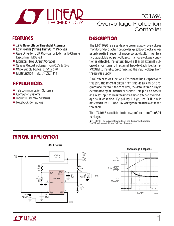
FEATURES DESCRIPTIO ±2% Overvoltage Threshold Accuracy The LTC®1696 is a standalone power supply overvoltage Low Profile (1mm) Thin SOTTM Package monitor and protection device designed to protect a power Gate Drive for SCR Crowbar or External N-Channel supply load in the event of an overvoltage fault. It monitors Disconnect MOSFET two adjustable output voltages. If an overvoltage condi- Monitors Two Output Voltages tion is detected, the output drives either an external SCR Senses Output Voltages from 0.8V to 24V crowbar or turns off external back-to-back N-channel Wide Supply Range: 2.7V to 27V MOSFETs, thereby, disconnecting the input voltage from Multifunction TIMER/RESET Pin the power supply.
Pin 6 offers three functions. By connecting a capacitor to APPLICATIO S this pin, the internal glitch filter time delay can be pro- grammed. Without the capacitor, the default time delay is
Telecommunication Systems
determined by an internal capacitor. This pin also serves
Computer Systems
as a reset input to clear the internal latch after an overvolt-
Industrial Control Systems
age fault condition. By pulling it high, the OUT pin is
Notebook Computers
activated if the FB1 and FB2 voltages remain below the trip threshold. The LTC1696 is available in the low profile (1mm) Thin SOT package. , LTC and LT are registered trademarks of Linear Technology Corporation. Thin SOT is a trademark of Linear Technology Corporation.
TYPICAL APPLICATIO
SCR Crowbar
Overvoltage Response
VOUT2 VCC POWER 5V
12V SUPPLY VOUT1
3.3V 0.5V/DIV
137k TIMER/RESET
1% 2V/DIV
TIMER/ FB1 RESET
RESETQ1
44.2k LTC1696 IOUT
1% 20m A/DIV
GND FB2
VCC OUT
100µs/DIV 1696 TA02
SCR C2 2N6507 0.1µF
1696 TA01
Page Summary Contents For LINEAR LTC1696 Data Sheet Manual
Manual Details
| Brand | Linear |
|---|---|
| Pages | 12 |
| File Size | 221.15 KB |
| Published | June 05, 2026 |
Enter the captcha to get the download link:

Frequently Asked Questions
What is the primary function of the LTC1696?
It monitors two adjustable output voltages, FB1 and FB2, to detect overvoltage faults and disconnects power.
How can I customize the glitch filter time delay?
You can program the internal glitch filter time delay by connecting a capacitor to the TIMER/RESET pin.
What are the operational supply voltage limits?
The unit operates across a minimum to maximum supply voltage range of 2.7V to 27V.
How does the LTC1696 protect against overvoltage?
It either drives an external SCR crowbar or turns off external back-to-back N-channel MOSFETs, disconnecting power.