LINEAR DN355f Data Sheet/Manual
Summary
Selecting optimal low-noise operational amplifiers is crucial for high-performance analog design. This comprehensive guide demystifies complex op amp noise principles, detailing how internal source noise, resistor thermal noise, and overall circuit impedance contribute to signal degradation. It provides engineers of all experience levels with structured graphs and calculation methods necessary to select the ideal component, ensuring ultra-low total input-referred noise for sensitive applications like active filters and transimpedance amplifiers.
Page 1 Text Content
advertisement
Op Amp Selection Guide for Optimum Noise Performance Design Note 355 Glen Brisebois
VNVR(EQ)
Introduction RS Linear Technology continues to add to its portfolio of low
noise op amps. This is not because the physics of noise has changed, but because low noise specifi cations are
being combined with new features such as rail-to-rail operation, shutdown, low voltage and low power opera- tion. Op amp noise is dependent on input stage operating
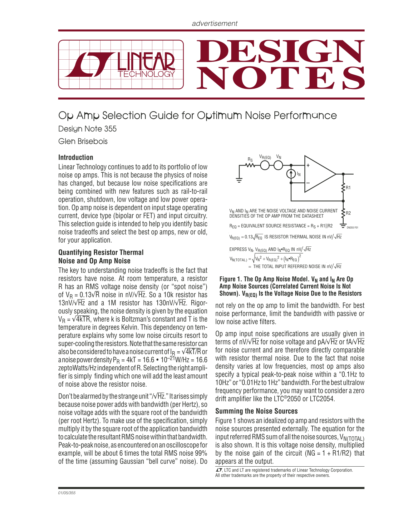
VN AND IN ARE THE NOISE VOLTAGE AND NOISE CURRENT
current, device type (bipolar or FET) and input circuitry. DENSITIES OF THE OP AMP FROM THE DATASHEET
This selection guide is intended to help you identify basic REQ = EQUIVALENT SOURCE RESISTANCE = RS + R1||R2
DN355 F01
noise tradeoffs and select the best op amps, new or old,
0.13 REQ Hz IS RESISTOR THERMAL NOISE IN
VR(EQ) n V
for your application.
Hz EXPRESS VN, VR(EQ) AND IN•REQ IN Quantifying Resistor Thermal n V
VN(TOTAL) VN VR(EQ) IN•REQ( )2
Noise and Op Amp Noise
Hz= THE TOTAL INPUT REFERRED NOISE IN n V
The key to understanding noise tradeoffs is the fact that resistors have noise. At room temperature, a resistor Figure 1. The Op Amp Noise Model. VN and IN Are Op
R has an RMS voltage noise density (or “spot noise”) Amp Noise Sources (Correlated Current Noise Is Not of VR = 0.13√⎯R noise in n V/√⎯H Shown). VR(EQ) Is the Voltage Noise Due to the Resistors
⎯z. So a 10k resistor has
13n V/√⎯H ⎯z and a 1M resistor has 130n V/√⎯H ⎯z. Rigor-
not rely on the op amp to limit the bandwidth. For best
ously speaking, the noise density is given by the equation
noise performance, limit the bandwidth with passive or
VR = √⎯4 ⎯k ⎯T⎯R, where k is Boltzman’s constant and T is the
low noise active fi lters.
temperature in degrees Kelvin. This dependency on tem-
Op amp input noise specifi cations are usually given in
perature explains why some low noise circuits resort to
terms of n V/√⎯H ⎯z for noise voltage and p A/√⎯H⎯z or f A/√⎯H ⎯z
super-cooling the resistors. Note that the same resistor can
for noise current and are therefore directly comparable
also be considered to have a noise current of IR = √⎯4⎯k⎯T/⎯R or
with resistor thermal noise. Due to the fact that noise
a noise power density PR = 4k T = 16.6 10–21W/Hz = 16.6
density varies at low frequencies, most op amps also
zepto Watts/Hz independent of R. Selecting the right ampli-
specify a typical peak-to-peak noise within a “0.1Hz to
fi er is simply fi nding which one will add the least amount
10Hz” or “0.01Hz to 1Hz” bandwidth. For the best ultralow
of noise above the resistor noise.
frequency performance, you may want to consider a zero
Don’t be alarmed by the strange unit “/√⎯H⎯z.” It arises simply
drift amplifi er like the LTC®2050 or LTC2054.
because noise power adds with bandwidth (per Hertz), so
noise voltage adds with the square root of the bandwidth Summing the Noise Sources (per root Hertz). To make use of the specifi cation, simply Figure 1 shows an idealized op amp and resistors with the multiply it by the square root of the application bandwidth noise sources presented externally. The equation for the to calculate the resultant RMS noise within that bandwidth. input referred RMS sum of all the noise sources, VN(TOTAL) Peak-to-peak noise, as encountered on an oscilloscope for is also shown. It is this voltage noise density, multiplied example, will be about 6 times the total RMS noise 99% by the noise gain of the circuit (NG = 1 + R1/R2) that of the time (assuming Gaussian “bell curve” noise). Do appears at the output. , LTC and LT are registered trademarks of Linear Technology Corporation. All other trademarks are the property of their respective owners.
Page Summary Contents For LINEAR DN355f Data Sheet/Manual
Manual Details
| Brand | Linear |
|---|---|
| Pages | 2 |
| File Size | 229.63 KB |
| Published | July 16, 2026 |
Enter the captcha to get the download link:
