# A B C D E F G H I J K L M N O P Q R S T U V W X Y Z

LINEAR LTC1968 User's Manual and Technical Data Sheet

Summary

The LTC1968 is a high-precision, wide bandwidth True RMS-to-DC converter designed for accurate measurement applications. It utilizes advanced Delta Sigma technology to ensure exceptional linearity and minimizes calibration complexity. The manual provides detailed electrical specifications, operational characteristics, and application examples for building demanding instruments such as digital multimeters and panel meters by delivering reliable, true RMS measurements across a wide range of inputs. (Approx. 400 characters)
📄 Preview PAGE OF 28

Page 1 Text Content

LTC1968

Precision Wide Bandwidth, RMS-to-DC Converter

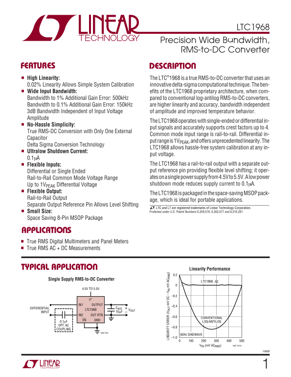
FEATURES DESCRIPTIO High Linearity: The LTC®1968 is a true RMS-to-DC converter that uses an 0.02% Linearity Allows Simple System Calibration innovative delta-sigma computational technique. The ben- Wide Input Bandwidth: efits of the LTC1968 proprietary architecture, when com- Bandwidth to 1% Additional Gain Error: 500k Hz pared to conventional log-antilog RMS-to-DC converters,

Bandwidth to 0.1% Additional Gain Error: 150k Hz are higher linearity and accuracy, bandwidth independent

3d B Bandwidth Independent of Input Voltage of amplitude and improved temperature behavior. Amplitude

The LTC1968 operates with single-ended or differential in-

No-Hassle Simplicity:

put signals and accurately supports crest factors up to 4.

True RMS-DC Conversion with Only One External

Common mode input range is rail-to-rail. Differential in-

Capacitor

put range is 1VPEAK, and offers unprecedented linearity. The

Delta Sigma Conversion Technology

LTC1968 allows hassle-free system calibration at any in-

Ultralow Shutdown Current:

put voltage.

Flexible Inputs: The LTC1968 has a rail-to-rail output with a separate out-

NE AR IT ER RO (V OU DC IN AC RM S)

Differential or Single Ended put reference pin providing flexible level shifting; it oper- Rail-to-Rail Common Mode Voltage Range ates on a single power supply from 4.5V to 5.5V. A low power Up to 1VPEAK Differential Voltage shutdown mode reduces supply current to 0.1µA.

Flexible Output:

The LTC1968 is packaged in the space-saving MSOP pack-

Rail-to-Rail Output

age, which is ideal for portable applications.

Separate Output Reference Pin Allows Level Shifting

, LTC and LT are registered trademarks of Linear Technology Corporation. Small Size: Protected under U.S. Patent Numbers 6,359,576, 6,362,677 and 6,516,291

Space Saving 8-Pin MSOP Package

APPLICATIO S True RMS Digital Multimeters and Panel Meters True RMS AC + DC Measurements

TYPICAL APPLICATIO Linearity Performance

Single Supply RMS-to-DC Converter

LTC1968, ∆Σ

4.5V TO 5.5V

V+ IN1 OUTPUT

DIFFERENTIAL CAVE

LTC1968 VOUT

INPUT 10µF

IN2 OUT RTN

CONVENTIONAL

EN GND

0.1µF LOG/ANTILOG OPT. AC

COUPLING

1968 TA01

60Hz SINEWAVE –1.0LI

VIN (m V ACRMS) 1968 TA01b

Page Summary Contents For LINEAR LTC1968 User's Manual and Technical Data Sheet

Page 1 LTC1968 Precision Wide Bandwidth, RMS-to-DC Converter FEATURES DESCRIPTIO High Linearity: The LTC®1968 is a true RMS-to-DC converter that uses an 0.02% Linearity Allows Simple System Calibration innov...
Page 2 LTC1968 ABSOLUTE AXI U RATI GS PACKAGE/ORDER I FOR ATIO (Note 1) Supply Voltage ORDER PART V+ to GND 6V NUMBER TOP VIEW Input Currents (Note 2) ±10m A GND ENABLE LTC1968CMS8 Output Current (Note 3) ±1...
Page 3 LTC1968 ELECTRICAL CHARACTERISTICS The ● denotes specifications which apply over the full operating temperature range, otherwise specifications are TA = 25°C. V+ = 5V, VOUTRTN = 2.5V, CAVE = 10µF, VIN...
Page 4 LTC1968 TYPICAL PERFOR A CE CHARACTERISTICS OFFSET VOLTAGE (m V) OFFSET VOLTAGE (m V) GA IN RR OR GA IN RR OR Gain and Offset Gain and Offset vs Input Common Mode Voltage vs Output Common Mode Voltage...
Page 5 SU PP LY UR RE NT (m A) {V OU TD |V IN DC (m V) OU TP UT OL TA GE (m DC LTC1968 TYPICAL PERFOR A CE CHARACTERISTICS Performance vs Crest Factor Performance vs Large Crest Factor AC Linearity 201.0 0.2...
Page 6 {V (m DC ) – (m } ( V) OU TP UT OL TA GE (m V) OU IN S) LTC1968 TYPICAL PERFOR A CE CHARACTERISTICS Input Common Mode Rejection Bandwidth to 500k Hz DC Transfer Function Near Zero Ratio vs Frequency 0...
Page 7 LTC1968 PI FU CTIO S GND (Pin 1): Ground. The power return pin. OUT RTN (Pin 6): Output Return. The output voltage is created relative to this pin. The VOUT and OUT RTN pins IN1 (Pin 2): Differential ...
Page 8 LTC1968 APPLICATIO S I FOR ATIO currents. The power delivered to the load depends on the the lowpass filter. The input to the LPF is the calculation firing angle, as well as any parasitic losses such ...
Page 9 LTC1968 APPLICATIO S I FOR ATIO Note that the internal scalings are such that the ∆Σ output duty cycle is limited to 0% or 100% only when VIN exceeds ±4 • VOUT. Linearity of an RMS-to-DC Converter VOU...
Page 10 LTC1968 DC RR OR APPLICATIO S I FOR ATIO Because this peak has energy (proportional to voltage lowest frequency signals of interest. For a single averaging squared) that is 16 times (42) the energy of...
Page 11 PE AK RR OR LTC1968 APPLICATIO S I FOR ATIO –0.2 –0.4 –0.6 INPUT FREQUENCY (Hz) Figure 8. Peak Error vs Input Frequency with One Cap Averaging because of the computation of the square of the input. Th...
Page 12 LTC1968 APPLICATIO S I FOR ATIO Input Connections work well with dual supply configurations, but in single supply configurations it will be necessary to raise the volt- The LTC1968 input is differenti...
Page 13 LTC1968 APPLICATIO S I FOR ATIO Output Connections For laboratory evaluation, it may suffice to use a bench-top DMM with the ability to disconnect the 10MΩ shunt. The LTC1968 output is differentially,...
Page 14 SE TT LI NG CC UR AC LTC1968 OU TP UT (m V) APPLICATIO S I FOR ATIO 100m V to 110m V (+10%) and back (–10%), the step But with 220µF, the settling time to even 10% is a full 10 responses are essential...
Page 15 LTC1968 APPLICATIO S I FOR ATIO Reducing Ripple with a Post Filter concern. To do this, tie all three ground symbols shown in Figure 12 to the signal reference, as well as to the differ- The output ri...
Page 16 LTC1968 APPLICATIO S I FOR ATIO somewhat lower (≈0.7 • 1.27 ≈ 0.9Hz) than with 10µF Figure 15 shows the step response of the same three cases alone. To adjust the bandwidth of either of them, simply w...
Page 17 PE AK RR OR PE AK RR OR LTC1968 APPLICATIO S I FOR ATIO –0.2 C = 100µF –0.4 –0.6 C = 47µF C = 22µF C = 10µF C = 4.7µF C = 2.2µF C = 0.47µF C = 0.22µF C = 0.1µFC =1µF INPUT FREQUENCY (Hz) Figure 16. Pe...
Page 18 SE TT LI NG CC UR AC SE TT LI NG CC UR AC LTC1968 APPLICATIO S I FOR ATIO SETTLING TIME (SEC) Figure 18. Settling Time with Buffered Post Filter SETTLING TIME (SEC) Figure 19. Settling Time with DC-Ac...
Page 19 LTC1968 APPLICATIO S I FOR ATIO waveform dynamics and the type of filtering used. The from) the voltage at the output. The conversion gain of the above method is conservative for some cases and about ...
Page 20 LTC1968 APPLICATIO S I FOR ATIO VOUT = (√(5m V AC)2 + (0.4m V DC)2) • 1.001 + 0.2m V Although there is a pattern to the response versus fre- = 5.221m V quency that repeats every sample frequency, the ...
Page 21 LTC1968 APPLICATIO S I FOR ATIO This allows each sample to settle to within 46ppm and it is Output Impedance these samples that are used to compute the RMS value. The LTC1968 output impedance during o...
Page 22 LTC1968 APPLICATIO S I FOR ATIO LTC1968 7106 TYPE SYSTEM CALIBRATION OUTPUT IN HI The LTC1968 static accuracy can be improved with end- OUT RTN IN LO system calibration. Traditionally, calibration has...
Page 23 LTC1968 APPLICATIO S I FOR ATIO The trade-off here is that on the one hand, the DC error is –full-scale input can be done by physically inverting the input frequency dependent, so a calibration signal...
Page 24 LTC1968 APPLICATIO S I FOR ATIO TROUBLESHOOTING GUIDE 4. Gain is low by a few percent, along with other screwy results. Top Ten LTC1968 Application Mistakes Probably tried to use output in a floating,...
Page 25 LTC1968 APPLICATIO S I FOR ATIO 7. Output is noisy with >200k Hz inputs. 10. Gain is low by ≅1% or more, no other problems. This is a fundamental characteristic of this topol- Probably due to circu...
Page 26 LTC1968 SI PLIFIED SCHE ATIC 2nd ORDER ∆Σ MODULATOR OUTPUT A2A1 C11 CAVE C4 C8 OUT RTN 1968 SS CLOSED DURING SHUTDOWN 50k EN BLEED RESISTOR FOR CAVE TO BIAS CONTROL TYPICAL APPLICATIO S 5V Single Supp...
Page 27 LTC1968 TYPICAL APPLICATIO S ±2.5V Supplies, Single Ended, DC-Coupled RMS-to-DC Converter with Shutdown RMS Noise Measurement VOLTAGE ≥2V NOISE IN OFF –2.5V 1m VDC ≤–2VON VOUT = 1µVRMS OF INPUT NOISE ...
Page 28 LTC1968 TYPICAL APPLICATIO Audio Amplitude Compressor ATTENUATE BY 1/4 V+ LT1256 VIN R15 R1 C1 R4 47Ω 100k 47n F 2.49k VOUT GAIN OF 4 A2 VC RC RFS VFS ATTENUATION CONTROL LT1636 200k LTC1968 1k VOUT I...

Manual Details

Brand Linear
Pages 28
File Size 291.48 KB
Published June 16, 2026
3 views

Enter the captcha to get the download link:

captcha

Frequently Asked Questions

What power supply range does the LTC1968 operate on?

It operates using a single power supply from 4.5V to 5.5V.

How low is the current consumption when the device is shut down?

The shutdown mode reduces the supply current to an ultralow level of 0.1µA.

Is this converter suitable for portable or space-constrained environments?

Yes, it features a rail-to-rail output and is packaged in a space-saving MSOP package.

Does the device allow for external voltage adjustment on the output?

It includes a separate output reference pin that provides flexible level shifting capabilities.