# A B C D E F G H I J K L M N O P Q R S T U V W X Y Z

LINEAR LTC1863 LTC1867 Data Sheet User's Manual

Summary

The LTC1863/LTC1867 is a high-performance 12-/16-bit, 8-channel Analog-to-Digital Converter (ADC) designed for demanding data acquisition systems. This manual provides comprehensive technical details on this ultra-low-power converter, which operates at up to 200ksps and features an internal multiplexer for complex signal conditioning. Ideal for industrial control, battery-operated devices, and imaging applications requiring high accuracy ($\approx$89dB SNR) and minimal power draw.
📄 Preview PAGE OF 16

Page 1 Text Content

查询LCD1863供应商

LTC1863/LTC1867 12-/16-Bit, 8-Channel 200ksps ADCs

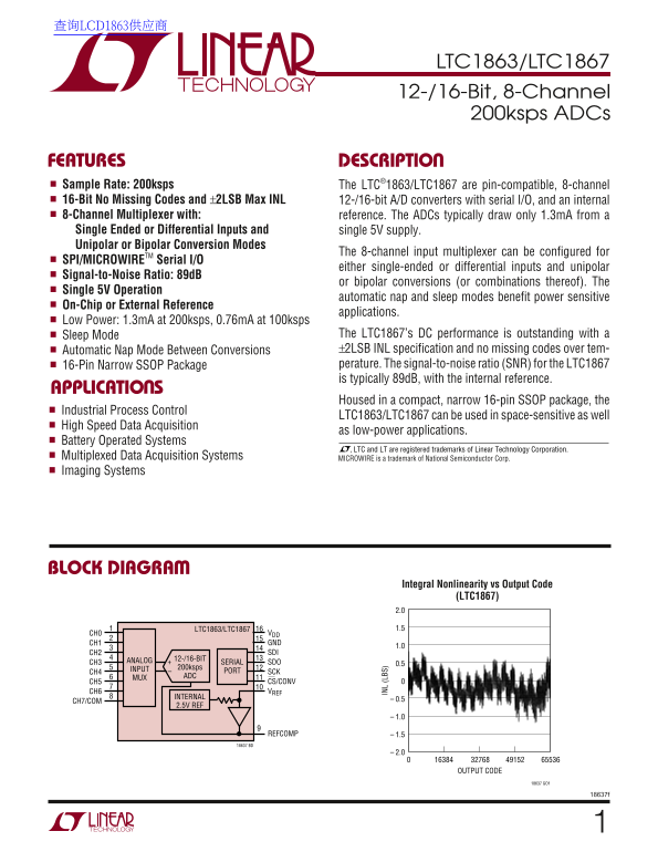
FEATURES DESCRIPTIO Sample Rate: 200ksps The LTC®1863/LTC1867 are pin-compatible, 8-channel 16-Bit No Missing Codes and ±2LSB Max INL 12-/16-bit A/D converters with serial I/O, and an internal 8-Channel Multiplexer with: reference. The ADCs typically draw only 1.3m A from a Single Ended or Differential Inputs and single 5V supply. Unipolar or Bipolar Conversion Modes

The 8-channel input multiplexer can be configured for

SPI/MICROWIRETM Serial I/O

either single-ended or differential inputs and unipolar

Signal-to-Noise Ratio: 89d B

or bipolar conversions (or combinations thereof). The

Single 5V Operation

automatic nap and sleep modes benefit power sensitive

On-Chip or External Reference

applications.

Low Power: 1.3m A at 200ksps, 0.76m A at 100ksps

Sleep Mode The LTC1867’s DC performance is outstanding with a Automatic Nap Mode Between Conversions ±2LSB INL specification and no missing codes over tem- 16-Pin Narrow SSOP Package perature. The signal-to-noise ratio (SNR) for the LTC1867 is typically 89d B, with the internal reference.

IN (L BS

APPLICATIO S

Housed in a compact, narrow 16-pin SSOP package, the

Industrial Process Control

LTC1863/LTC1867 can be used in space-sensitive as well

High Speed Data Acquisition

as low-power applications.

Battery Operated Systems

, LTC and LT are registered trademarks of Linear Technology Corporation.

Multiplexed Data Acquisition Systems MICROWIRE is a trademark of National Semiconductor Corp. Imaging Systems

BLOCK DIAGRA

Integral Nonlinearity vs Output Code

(LTC1867)

LTC1863/LTC1867 1.5

CH0 VDD CH1 GND

CH2 SDI

ANALOG 12-/16-BIT

CH3 SERIAL SDO 0.5

INPUT 200ksps

CH4 PORT SCK

MUX ADC

CH5 CS/CONV CH6 VREF

INTERNAL

CH7/COM 0.5

2.5V REF

REFCOMP 1.5

18637 BD

OUTPUT CODE

18637 GO1

Page Summary Contents For LINEAR LTC1863 LTC1867 Data Sheet User's Manual

Page 1 查询LCD1863供应商 LTC1863/LTC1867 12-/16-Bit, 8-Channel 200ksps ADCs FEATURES DESCRIPTIO Sample Rate: 200ksps The LTC®1863/LTC1867 are pin-compatible, 8-channel 16-Bit No Missing Codes and ±2LSB Max INL 12...
Page 2 LTC1863/LTC1867 ABSOLUTE AXI RATI GS PACKAGE/ORDER I FOR ATIO (Notes 1, 2) TOP VIEW ORDER PART Supply Voltage (VDD) –0.3V to 6V NUMBER CH0 VDD Analog Input Voltage CH1 GND LTC1863CGN CH0-CH7/COM (Note...
Page 3 LTC1863/LTC1867 DY A IC ACCURACY (Note 5) LTC1863 LTC1867/LTC1867A SYMBOL PARAMETER CONDITIONS MIN TYP MAX MIN TYP MAX UNITS THD Total Harmonic Distortion 1k Hz Input Signal, Up to 5th Harmonic –94.5 ...
Page 4 LTC1863/LTC1867 POWER REQUIRE E TS The ● denotes the specifications which apply over the full operating temperature range, otherwise specifications are at TA = 25°C. (Note 5) LTC1863/LTC1867/LTC1867A ...
Page 5 AM PL IT UD (d B) AM PL IT UD (d B) IN (L SB LTC1863/LTC1867 TYPICAL PERFOR A CE CHARACTERISTICS (LTC1867) Integral Nonlinearity vs Differential Nonlinearity vs Output Code Output Code Histogram for 4...
Page 6 SU PP LY UR RE NT (m A) LTC1863/LTC1867 TYPICAL PERFOR A CE CHARACTERISTICS (LTC1863/LTC1867) Supply Current vs f SAMPLE Supply Current vs Supply Voltage IN (L BS Supply Current vs Temperature VDD = 5...
Page 7 LTC1863/LTC1867 PI FU CTIO S CHO-CH7/COM (Pins 1-8): Analog Input Pins. Analog SCK (Pin 12): Shift Clock. This clock synchronizes the inputs must be free of noise with respect to GND. CH7/ serial data...
Page 8 LTC1863/LTC1867 TI I G DIAGRA S t1 (For Short Pulse Mode) t2 (SDO Valid Before SCK↑), t3 (SDO Valid Hold Time After SCK↓)t1 CS/CONV SCK50%50% 2.4V 0.4VSDO t5 (SDI Setup Time Before SCK↑), t4 (SDO Vali...
Page 9 LTC1863/LTC1867 APPLICATIO S I FOR ATIO Analog Input Multiplexer Changing the MUX Assignment “On the Fly” 1st Conversion 2nd Conversion The analog input multiplexer is controlled by a 7-bit input data...
Page 10 LTC1863/LTC1867 APPLICATIO S I FOR ATIO Driving the Analog Inputs The analog inputs of the LTC1863/LTC1867 are easy to LT1360 - 37MHz voltage feedback amplifier. 3.8m A sup- drive. Each of the analog ...
Page 11 LTC1863/LTC1867 CO UN TS APPLICATIO S I FOR ATIO 50ΩANALOG Dynamic Performance INPUT LTC1863/ FFT (Fast Fourier Transform) test techniques are used to LTC1867 test the ADC’s frequency response, distor...
Page 12 LTC1863/LTC1867 APPLICATIO S I FOR ATIO where V1 is the RMS amplitude of the fundamental fre- Digital Interface quency and V2 through VN are the amplitudes of the The LTC1863/LTC1867 have very simple ...
Page 13 LTC1863/LTC1867 APPLICATIO S I FOR ATIO If the CS/CONV returns low during a bit decision, it can All analog inputs should be screened by GND. VREF, create a small error. For best performance ensure th...
Page 14 LTC1863/LTC1867 APPLICATIO S I FOR ATIO OU TP UT OD (T O’ CO PL IM EN T) CS/CONV t ACQ NOT NEEDED FOR LTC1863 SDI 0S S1 S0SD COM UNI SLP DON'T CAREDON'T CARE t CONV SDO MSB = D11 D10 D9 D8 D7 D6 D5 D4...
Page 15 LTC1863/LTC1867 PACKAGE DESCRIPTIO GN Package 16-Lead Plastic SSOP (Narrow .150 Inch) (Reference LTC DWG # 05-08-1641) .009 (0.229) REF .254 MIN .150 – .165 .0015 .0250 BSC.0165 ± RECOMMENDED SOLDER P...
Page 16 LTC1863/LTC1867 RELATED PARTS PART NUMBER DESCRIPTION COMMENTS LTC1417 14-Bit, 400ksps Serial ADC 20m W, Unipolar or Bipolar, Internal Reference, SSOP-16 Package LT1460 Micropower Precision Series Ref...

Manual Details

Brand Linear
Pages 16
File Size 333.88 KB
Published May 29, 2026
71 views

Enter the captcha to get the download link:

captcha

Frequently Asked Questions

What is the typical Signal-to-Noise Ratio (SNR) of this ADC at 1kHz?

The typical SNR provided is 89 dB for LTC1867/LTC1863.

Can the device handle both bipolar and unipolar signal conversions?

Yes, it supports Unipolar Mode (0-4.096V) as well as Bipolar Model inputs (-2.048V).

What are the standard operating temperature limits for this chip?

The specified operating range is 0°C to 70°C, although certain packages support –40°C to 85°C.

How does the device handle multiple input channels?

It includes an internal multiplexer that can configure inputs from Analog (CH0-CH7/COM) and Digital signals.